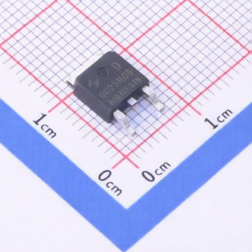
Specifications
Configuration :
Common Drain
Drain to Source Voltage :
20V
Current - Continuous Drain(Id) :
10A
RDS(on) :
11mΩ@2.5V,3A
Operating Temperature - :
-55℃~+150℃
Gate Threshold Voltage (Vgs(th)) :
1V@250uA
Type :
N-Channel
Reverse Transfer Capacitance (Crss@Vds) :
51pF
Number :
2 N-Channel
Output Capacitance(Coss) :
193pF
Input Capacitance(Ciss) :
1.258nF
Pd - Power Dissipation :
2W
Gate Charge(Qg) :
15nC@4.5V
Description :
N-Channel Array 20V 10A 2W Surface Mount TSSOP-8
Mfr. Part # :
CJS9004A
Model Number :
CJS9004A
Package :
TSSOP-8
Description

Product Overview

The CJS9004A is a Dual N-Channel MOSFET utilizing advanced trench technology, offering excellent RDS(ON) and low gate charge. It features ESD protection and is suitable for uni-directional or bi-directional load switch applications due to its common-drain configuration. This device is packaged in a TSSOP8.

Product Attributes

  • Brand: JIANGSU CHANGJING ELECTRONICS TECHNOLOGY CO., LTD
  • Device Code: S9004
  • Packaging: TSSOP8
  • Molding Compound: Green (if solid dot present)

Technical Specifications

ParameterSymbolTest ConditionMinTypMaxUnit
Drain-source breakdown voltageV(BR)DSSVGS = 0V, ID =250A20V
Zero gate voltage drain currentIDSSVDS =16V,VGS = 0V1A
Gate-body leakage currentIGSSVGS =4.5V, VDS = 0V1A
Gate-body leakage currentIGSSVGS =8V, VDS = 0V10A
Gate threshold voltageVGS(th)VDS =VGS, ID =250A0.41.0V
Drain-source on-resistanceRDS(on)VGS =4.5V, ID =3A6.07.0m
VGS =4.0V, ID =3A7.58.0m
VGS =3.8V, ID =3A8.59.0m
VGS =3.1V, ID =3A9.710.5m
VGS =2.5V, ID =3A11.011.5m
Diode forward voltageVSDIS =3A, VGS = 0V0.851.2V
Input CapacitanceCissVDS =10V,VGS =0V,f =0.1MHz193pF
Output CapacitanceCossVDS =10V,VGS =0V,f =0.1MHz51pF
Reverse Transfer CapacitanceCrssVDS =10V,VGS =0V,f =0.1MHzpF
Total gate chargeQgVDS =10V,VGS =4.5V,ID =7A15nC
Gate-source chargeQgsVDS =10V,VGS =4.5V,ID =7A3.4nC
Gate-drain chargeQg dVDS =10V,VGS =4.5V,ID =7A5.7nC
Turn-on delay timetd(on)VGS=4.5V,VDD=10V, RL=1.35,RGEN=330ns
Turn-on rise timetrVGS=4.5V,VDD=10V, RL=1.35,RGEN=354ns
Turn-off delay timetd(off)VGS=4.5V,VDD=10V, RL=1.35,RGEN=377ns
Turn-off fall timetfVGS=4.5V,VDD=10V, RL=1.35,RGEN=358ns
Maximum Ratings: Drain-Source VoltageVDS20V
Maximum Ratings: Gate-Source VoltageVGS12V
Maximum Ratings: Continuous Drain CurrentIDTa=2510A
Maximum Ratings: Pulsed Drain CurrentIDMTa=2550A
Maximum Ratings: Power DissipationPDTa=252.0W
Maximum Ratings: Thermal Resistance Junction to AmbientRJATa=2562.5/W
Maximum Ratings: Operating Junction and Storage TemperatureTJ, Tstg-55+150

2409301804_JSCJ-CJS9004A_C19268983.pdf

Send your message to this supplier
Send Now

Low RDS On Dual N Channel MOSFET JSCJ CJS9004A Suitable for Uni Directional and Bi Directional Loads

Ask Latest Price
Configuration :
Common Drain
Drain to Source Voltage :
20V
Current - Continuous Drain(Id) :
10A
RDS(on) :
11mΩ@2.5V,3A
Operating Temperature - :
-55℃~+150℃
Gate Threshold Voltage (Vgs(th)) :
1V@250uA
Contact Supplier
Low RDS On Dual N Channel MOSFET JSCJ CJS9004A Suitable for Uni Directional and Bi Directional Loads

Hefei Purple Horn E-Commerce Co., Ltd.

Verified Supplier
1 Years
anhui, hefei
Since 2009
Business Type :
Manufacturer, Distributor/Wholesaler, Agent, Importer
Employee Number :
300~500
Certification Level :
Verified Supplier
Contact Supplier
Submit Requirement