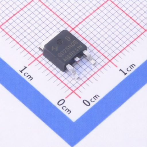
Specifications
Drain to Source Voltage :
20V
Current - Continuous Drain(Id) :
4A
RDS(on) :
50mΩ@4.5V,4A
Gate Threshold Voltage (Vgs(th)) :
1V
Type :
P-Channel
Reverse Transfer Capacitance (Crss@Vds) :
160pF
Number :
1 P-Channel
Output Capacitance(Coss) :
205pF
Input Capacitance(Ciss) :
1.45nF
Pd - Power Dissipation :
350mW
Gate Charge(Qg) :
17.2nC@4.5V
Description :
P-Channel 20V 4A 350mW Surface Mount SOT-23
Mfr. Part # :
CJ3415 R15
Model Number :
CJ3415 R15
Package :
SOT-23
Description

CJ3415 P-Channel MOSFET

The CJ3415 is a P-Channel MOSFET in a SOT-23 package, designed for load switching and PWM applications. It features excellent RDS(ON), low gate charge, and low gate voltages, making it suitable for efficient power management.

Product Attributes

  • Brand: JIANGSU CHANGJIANG ELECTRONICS TECHNOLOGY CO., LTD
  • Package Type: SOT-23

Technical Specifications

Parameter Symbol Test Condition Min Typ Max Unit
Maximum Ratings (Ta=25 unless otherwise noted)
Drain-Source Voltage VDS -20 V
Gate-Source Voltage VGS ±8 V
Continuous Drain Current (t≤10s) ID -4.0 A
Maximum Power Dissipation (t≤10s) PD 0.35 W
Thermal Resistance from Junction to Ambient RθJA 357 °C/W
Operating Junction Temperature TJ 150 °C
Storage Temperature TSTG -55 ~+150 °C
Static Parameters (Ta=25 °C unless otherwise specified)
Drain-source breakdown voltage V(BR)DSS VGS = 0V, ID =-250µA -20 V
Gate threshold voltage VGS(th) VDS =VGS, ID =-250µA -0.3 -0.56 -1 V
Gate-body leakage current IGSS VDS =0V, VGS =±8V ±10 ±1 µA
Zero gate voltage drain current IDSS VDS =-16V, VGS =0V -1 µA
Drain-source on-state resistance(note1) RDS(on) VGS =-4.5V, ID =-4A 0.037 0.050 Ω
VGS =-2.5V, ID =-4A 0.045 0.060
VGS =-1.8V, ID =-2A 0.056 0.073
Forward transconductance(note2) gFS VDS =-5V, ID =-4A 8 S
Body diode voltage(note2) VSD IS=-1A,VGS =0V -1 V
Dynamic Parameters (note3)
Input capacitance Ciss VDS =-10V,VGS =0V,f =1MHz 1450 pF
Output capacitance Coss 205
Reverse transfer capacitance Crss 160
Gate resistance Rg VDS =0V,VGS =0V,f =1MHz 6.5 Ω
Switching Parameters (note3)
Total gate charge Qg VDS =-10V,VGS =-4.5V,ID =-4A 17.2 nC
Gate-Source charge Qgs 1.3
Gate-drain charge Qgd 4.5
Turn-on delay time(note3) td(on) VDS=-10V, VGS=-4.5V RGEN =3Ω, RL=2.5Ω 9.5 ns
Turn-on rise time(note3) tr 17
Turn-off delay time(note3) td(off) 94
Turn-off fall time(note3) tf 35

2410121342_JSCJ-CJ3415-R15_C77896.pdf

Send your message to this supplier
Send Now

P Channel MOSFET SOT 23 Package Featuring JSCJ CJ3415 R15 Suitable for Load Switching Applications

Ask Latest Price
Drain to Source Voltage :
20V
Current - Continuous Drain(Id) :
4A
RDS(on) :
50mΩ@4.5V,4A
Gate Threshold Voltage (Vgs(th)) :
1V
Type :
P-Channel
Reverse Transfer Capacitance (Crss@Vds) :
160pF
Contact Supplier
P Channel MOSFET SOT 23 Package Featuring JSCJ CJ3415 R15 Suitable for Load Switching Applications

Hefei Purple Horn E-Commerce Co., Ltd.

Verified Supplier
1 Years
anhui, hefei
Since 2009
Business Type :
Manufacturer, Distributor/Wholesaler, Agent, Importer
Employee Number :
300~500
Certification Level :
Verified Supplier
Contact Supplier
Submit Requirement