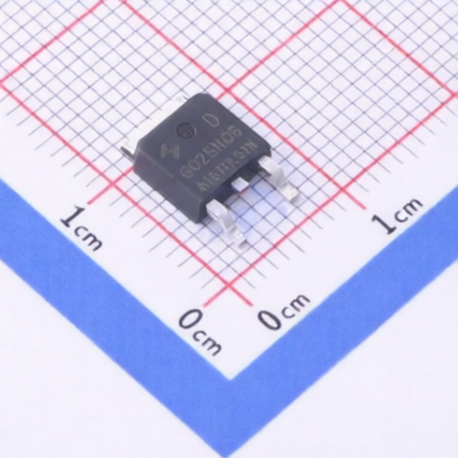
These miniature surface mount MOSFETs utilize High Cell Density process. Low RDS(on) assures minimal power loss and conserves energy, making this device ideal for use in power management circuitry. Typical applications are lower voltage application, power management in portable and battery-powered products such as computers, printers, and PCMCIA cards, cellular and cordless telephones.
| Parameter | Symbol | Test Condition | Min | Typ | Max | Unit |
| Drain-Source Voltage | VDS | -30 | V | |||
| Gate-Source Voltage | VGS | ±12 | V | |||
| Continuous Drain Current | ID | TA=25oC | -4.2 | A | ||
| Continuous Drain Current | ID | TA=70oC | -3.5 | A | ||
| Pulsed Drain Current | IDM | -30 | A | |||
| Continuous Source Current (Diode Conduction) | Is | TA=25oC | -2.2 | A | ||
| Power Dissipation | PD | TA=25oC | 1.38 | W | ||
| Liner Derating Factor | 0.01 | W/°C | ||||
| Operation Junction and Storage Temperature Range | TJ, Tstg | -55 | 150 | °C | ||
| Maximum Junction-to-Ambient | RTHJA | TA=25oC | 90 | °C/W | ||
| Drain-Source Breakdown Voltage | BVDSS | VGS=0V, ID=-250uA | -30 | V | ||
| Gate-Threshold Voltage | VGS(th) | VDS = VGS, ID = 250uA | -0.5 | -1.2 | V | |
| Gate-Body Leakage | IGSS | VDS = 0 V, VGS =±12V | ±100 | nA | ||
| Zero Gate Voltage Drain Current | IDSS | VDS = -24 V, VGS = 0 V, TJ = 25oC | -1 | uA | ||
| Zero Gate Voltage Drain Current | IDSS | VDS = -24 V, VGS = 0 V, TJ = 55oC | -5 | uA | ||
| Drain-Source On-Resistance | RDS(on) | VGS = -10 V, ID = -4.2 A | 43 | 50 | mΩ | |
| Drain-Source On-Resistance | RDS(on) | VGS = -4.5 V, ID = -4.0 A | 50 | 65 | mΩ | |
| Drain-Source On-Resistance | RDS(on) | VGS = -2.5 V, ID = -1.0A | 70 | 96 | mΩ | |
| Forward Transconductance | gfs | VDS = -5V, ID = -5A | 11 | S | ||
| Diode Forward Voltage | VSD | IS = -1.0 A, VGS = 0 V | -1.0 | V | ||
| Reverse Recovery Time | Trr | IS =-4A,VGS=0V, di/dt=100A/uS | 20.2 | nS | ||
| Reverse Recovery Charge | Qrr | 11.2 | nC | |||
| Total Gate Charge | Qg | VDS = -15V, VGS = -4.5V, ID = -4A | 9.4 | 16 | nC | |
| Turn-On Delay Time | td(on) | VDS=-15V, RL=3.6Ω,RG = 6Ω, VGS = -10V | 6.3 | 13 | ns | |
| Turn-On Rise Time | tr | 3.2 | 8.4 | |||
| Turn-Off Delay Time | td(off) | 38.2 | 48.5 | |||
| Turn-Off Fall Time | tf | 12 | 21.3 | |||
| Input Capacitance | Ciss | VGS=0V,VDS=-15V,f =1.0MHz | 954 | 1104 | pF | |
| Output Capacitance | Coss | 115 | 187 | |||
| Reverse Transfer Capacitance | Crss | 77 | 97 | |||
| Gate Resistance | Rg | f =1.0MHz | 6 | Ω |