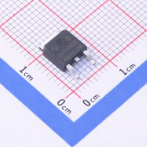
The SVDZ24NT is an N-channel enhancement mode power MOS field-effect transistor manufactured using Silan's new planar VDMOS process. It features an improved planar stripe cell and guard ring terminal designed to minimize on-state resistance, enhance switching performance, and provide superior withstand capability for high energy pulses in avalanche and commutation modes. This device is widely utilized in electrical ballast and low power switching power supply applications.
| Characteristics | Symbol | SVDZ24NT | SVDZ24ND | Unit |
| ABSOLUTE MAXIMUM RATINGS | ||||
| Drain-Source Voltage | VDS | 55 | 55 | V |
| Gate-Source Voltage | VGS | ±20 | ±20 | V |
| Drain Current (TC=25°C) | ID | 17 | 17 | A |
| Drain Current (TC=100°C) | ID | 12 | 12 | A |
| Drain Current Pulsed | IDM | 68 | 68 | A |
| Power Dissipation (TC=25°C) | PD | 45 | 45 | W |
| Derate above 25°C | 0.36 | 0.36 | W/°C | |
| Single Pulsed Avalanche Energy (Note 1) | EAS | 122 | 122 | mJ |
| Operation Junction Temperature Range | TJ | -55+175 | -55+175 | °C |
| Storage Temperature Range | Tstg | -55+175 | -55+175 | °C |
| THERMAL CHARACTERISTICS | ||||
| Thermal Resistance, Junction-to-Case | RθJC | 2.78 | 3.2 | °C/W |
| Thermal Resistance, Junction-to-Ambient | RθJA | 62.5 | 62 | °C/W |
| ELECTRICAL CHARACTERISTICS | ||||
| Drain -Source Breakdown Voltage | BVDSS | 55 | 55 | V |
| Drain-Source Leakage Current | IDSS | -- | 20 | µA |
| Gate-Source Leakage Current | IGSS | -- | ±100 | nA |
| Gate Threshold Voltage | VGS(th) | 2.0 -- 4.0 | 2.0 -- 4.0 | V |
| Static Drain-Source On State Resistance | RDS(on) | 45 (typ.) | 45 (typ.) | mΩ |
| Input Capacitance | Ciss | 400 (typ.) | 400 (typ.) | pF |
| Output Capacitance | Coss | 130 (typ.) | 130 (typ.) | pF |
| Reverse Transfer Capacitance | Crss | 12.5 (typ.) | 12.5 (typ.) | pF |
| Turn-on Delay Time | td(on) | 5.4 (typ.) | 5.4 (typ.) | ns |
| Turn-on Rise Time | tr | 32.5 (typ.) | 32.5 (typ.) | ns |
| Turn-off Delay Time | td(off) | 22.1 (typ.) | 22.1 (typ.) | ns |
| Turn-off Fall Time | tf | 12.4 (typ.) | 12.4 (typ.) | ns |
| Total Gate Charge | Qg | 10.5 (typ.) | 10.5 (typ.) | nC |
| Gate-Source Charge | Qgs | 2.5 (typ.) | 2.5 (typ.) | nC |
| Gate-Drain Charge | Qg d | 4.0 (typ.) | 4.0 (typ.) | nC |
| SOURCE-DRAIN DIODE RATINGS AND CHARACTERISTICS | ||||
| Continuous Source Current | IS | 17 | 17 | A |
| Pulsed Source Current | ISM | 68 | 68 | A |
| Diode Forward Voltage | VSD | 1.3 (typ.) | 1.3 (typ.) | V |
| Reverse Recovery Time | Trr | 43 (typ.) | 43 (typ.) | ns |
| Reverse Recovery Charge | Qrr | 0.05 (typ.) | 0.05 (typ.) | µC |