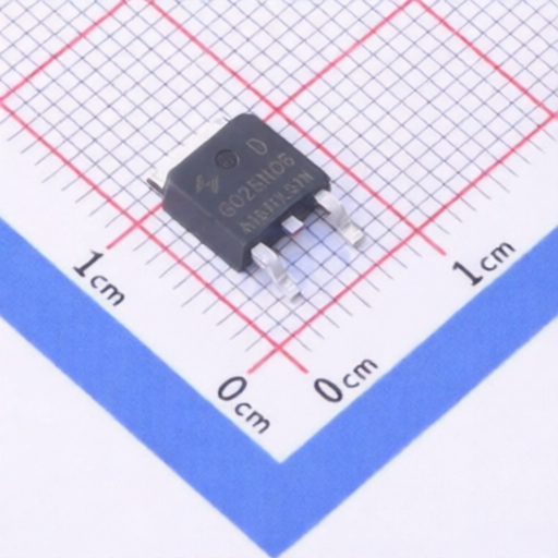
The BRCS045N08SHBD is an N-channel MOSFET in a TO-263 plastic package, designed for high-performance applications. It features a Drain-Source Voltage (VDS) of 80V and a continuous Drain Current (ID) of 155A at 25. This HF product is suitable for use in boost converters and synchronous rectifiers for consumer, telecom, and industrial power supplies, as well as LED backlighting. Key electrical characteristics include a low Static Drain-Source On-Resistance (RDS(on)) of 4.5m at 10V (typical 3.5m) and 9.0m at 6V (typical 4.7m). The device is RoHS compliant (Halogen-Free Product).
| Parameter | Symbol | Rating/Test Conditions | Value | Unit |
|---|---|---|---|---|
| Absolute Maximum Ratings (Ta=25) | ||||
| Drain-Source Voltage | VDSS | 80 | V | |
| Drain Current | ID(Tc=25) | 155 | A | |
| Pulsed Drain Current | IDM | 322 | A | |
| Gate-Source Voltage | VGS | 20 | V | |
| Single Pulsed Avalanche Energy (L=0.5mH) | EAS | 986 | mJ | |
| Avalanche Current | IAS | 43 | A | |
| Total Power Dissipation | PD(Tc=25) | 200 | W | |
| Junction and Storage Temperature Range | TJ,TSTG | -55 to 150 | ||
| Thermal Resistance-Junction to Ambient Steady-State | RJA | 62.5 | /W | |
| Thermal Resistance-Junction to Case Steady-State | RJC | 0.63 | /W | |
| Electrical Characteristics (Ta=25) | ||||
| Drain-Source Breakdown Voltage | BVDSS | VGS=0V, ID=250A | 80 (Min) / 92.5 (Typ) | V |
| Zero Gate Voltage Drain Current | IDSS | VDS=80V, VGS=0V | 1 | A |
| Gate-Body Leakage Current | IGSS | VGS=20V, VDS=0V | 100 | nA |
| Gate Threshold Voltage | VGS(th) | VDS=VGS, ID=250A | 2 (Min) / 3 (Typ) / 4 (Max) | V |
| Static Drain-Source On-Resistance | RDS(on) | VGS=10V, ID=20A | 3.5 (Typ) / 4.5 (Max) | m |
| Static Drain-Source On-Resistance | RDS(on) | VGS=6V, ID=10A | 4.7 (Typ) / 9.0 (Max) | m |
| Forward On Voltage | VSD | VGS=0V, IS=1A | 1.4 | V |
| Gate resistance | Rg | f=1MHz | 1 | |
| Input Capacitance | Ciss | VDS=25V, VGS=0V, f=1MHz | 4240 | pF |
| Output Capacitance | Coss | VDS=25V, VGS=0V, f=1MHz | 2550 | pF |
| Reverse Transfer Capacitance | Crss | VDS=25V, VGS=0V, f=1MHz | 150 | pF |
| Total Gate Charge | Qg | VGS=10V, VDS=40V, ID=20A | 73 | nC |
| Gate Source Charge | Qgs | VGS=10V, VDS=40V, ID=20A | 19.2 | nC |
| Gate Drain Charge | Qgd | VGS=10V, VDS=40V, ID=20A | 12 | nC |
| Turn-On Delay Time | td(on) | VGS=10V, VDS=40V, RL=2, RGEN=3 | 19 | ns |
| Turn-On Rise Time | tr | VGS=10V, VDS=40V, RL=2, RGEN=3 | 12.5 | ns |
| Turn-Off Delay Time | td(off) | VGS=10V, VDS=40V, RL=2, RGEN=3 | 40 | ns |
| Turn-Off Fall Time | tf | VGS=10V, VDS=40V, RL=2, RGEN=3 | 8 | ns |