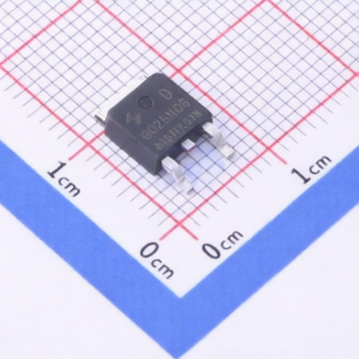
Product Overview
The AW3112 is a 30V PNP power bipolar transistor integrated with a 20V trench NMOSFET, functioning as a base switch. Manufactured using planar epitaxial process technology, it offers a low collector-emitter saturation voltage and high current gain, making it particularly suitable for high-current linear charging of lithium batteries. The device is available in a compact DFN2X2-6L package and operates within a temperature range of -40 to +150. Key applications include battery charging and power management for portable electronic devices.
Product Attributes
- Brand: Shanghai A-Power Electronics Technology Co., Ltd.
- Certifications: ROHS compliant
Technical Specifications
| Model | Operating Temperature Range | Package Type | Device Marking | Delivery Form |
| AW3112DNR | -40~150 | DFN2X2-6L | AW12 | Tape & Reel (3000 pcs/) |
| Parameter | Rating | Unit |
| 30V PNP BJT Absolute Maximum Ratings |
| Collector-Base Voltage (Vcbo) | -40 | V |
| Collector-Emitter Voltage (Vceo) | -32 | V |
| Emitter-Base Voltage (Vebo) | -6 | V |
| Collector Current (Ic) | -3 | A |
| Collector Peak Current (Icm) | -6 | A |
| 20V NMOSFET Absolute Maximum Ratings |
| Drain-Source Voltage (Vdss) | 20 | V |
| Gate-Source Voltage (Vgss) | 8 | V |
| Drain Current (Id) | 180 | mA |
| Drain Peak Current (Idp) | 360 | mA |
| Temperature, Power Dissipation, and Thermal Resistance |
| Power Dissipation (Ptot) | 1.5 | W |
| Junction Temperature (Tj) | 150 | |
| Storage Temperature (Tstg) | -65~150 | |
| Lead Temperature (Tl) | 260 | |
| Thermal Resistance Coefficient ( JA) | 85.6 | /W |
| Symbol | Parameter | Test Conditions | Min | Typical | Max | Unit |
| 30V PNP BJT Electrical Characteristics (T=25 unless otherwise specified) |
| BVceo | Collector-Emitter Breakdown Voltage | Ic=-10mA, Ib=0mA | -32 | | | V |
| BVcbo | Collector-Base Breakdown Voltage | Ic=-0.1mA, Ie=0mA | -40 | | | V |
| BVebo | Emitter-Base Breakdown Voltage | Ie=-1mA, Ic=0mA | -6 | | | V |
| Icbo | Collector Leakage Current | Vcb=-30V | | -0.1 | | uA |
| Iebo | Emitter Leakage Current | Veb=-5V | | -0.1 | | uA |
| Vce(sat) | Collector-Emitter Saturation Voltage | Ic=-1A, Ib=-20mA | | -0.35 | | V |
| Vbe(sat) | Base-Emitter Saturation Voltage | Ic=-1A, Ib=-20mA | | -1.2 | | V |
| HFE1 | DC Current Gain (High Current) | Ic=-1A, Vce=-2V | 100 | | | |
| HFE2 | DC Current Gain (Low Current) | Ic=-0.1A, Vce=-2V | 200 | | | |
| 20V NMOSFET Electrical Characteristics (T=25 unless otherwise specified) |
| BVdss | Drain-Source Breakdown Voltage | Vgs=0V, Ids=250uA | 20 | | | V |
| Vth | Threshold Voltage | Vgs=Vds, Ids=250uA | 0.4 | 1.0 | | V |
| Igss | Gate Leakage Current | Vds=0V, Vgs=8V | | 100 | | nA |
| Idss | Drain Leakage Current | Vgs=0V, Vds=20V | | 1 | | uA |
| Rds(on) | Drain-Source On-Resistance | Vgs=2.5V, Id=50mA | | 0.5 | | |
| Rds(on) | Drain-Source On-Resistance | Vgs=1.5V, Id=50mA | | 1 | | |
| Vsd | Body Diode Forward Voltage | Isd=1A, Vgs=0V | 0.5 | 1.2 | | V |
| Symbol | Dimensions | Unit |
| DFN2X2-6L Package Dimensions |
| A | 0.700 - 0.750 - 0.800 | mm |
| A1 | 0.000 - 0.025 - 0.050 | mm |
| A3 | 0.203 REF | |
| D | 1.924 - 2.000 - 2.076 | mm |
| E | 1.924 - 2.000 - 2.076 | mm |
| D1 | 0.850 - 0.950 - 1.050 | mm |
| E1 | 0.700 - 0.800 - 0.900 | mm |
| D2 | 0.200 - 0.300 - 0.400 | mm |
| E2 | 0.700 - 0.800 - 0.900 | mm |
| e1 | 0.650 TYP | |
| e2 | 0.325 TYP | |
| k | 0.200 MIN | |
| b | 0.250 - 0.300 - 0.350 | mm |
| e | 0.650 TYP | |
| L | 0.300 - 0.350 - 0.400 | mm |
2511110935_AWINIC-Shanghai-Awinic-Tech-AW3112DNR_C498339.pdf