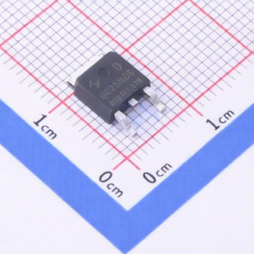
The BCW120N160W1 is a high-performance N-Channel Silicon Carbide Power MOSFET designed for demanding power electronic applications. It offers a combination of high blocking voltage, low on-resistance, and high-speed switching capabilities, making it suitable for solar inverters, switch mode power supplies, high voltage DC/DC converters, battery chargers, motor drives, and pulsed power applications. Key benefits include higher system efficiency, reduced cooling requirements, increased power density, and the ability to operate at increased system switching frequencies.
| Symbol | Parameter | Test Conditions | Value | Unit |
|---|---|---|---|---|
| VDSmax | Drain - Source Voltage | VGS=0V, ID=100A | 1200 | V |
| VGSmax | Gate - Source Voltage | Absolute maximum values | -8 / +22 | V |
| VGSop | Gate - Source Voltage | Recommended operational values | -5 / +18 | V |
| ID | Continuous Drain Current | VGS=18V, TC=25C | 22 | A |
| ID | Continuous Drain Current | VGS=18V, TC=100C | 16 | A |
| IDM | Pulse Drain Current | Pulse width limited by Tjmax | 58 | A |
| TJ, TSTG | Operating Junction and Storage Temperature | -55 to 175 | C | |
| RJC | Thermal Resistance, Junction to Case, Max. | 1.19 | /W | |
| RJA | Thermal Resistance, Junction to Ambient, Max. | 27.47 | /W | |
| Tsold | Soldering temperature, wave soldering only allowed at leads | 260 | ||
| BVDSS | Drain to Source Breakdown Voltage | VGS = 0 V, ID=100 A | 1200 | V |
| VGS(th) | Gate Threshold Voltage | VGS = VDS, ID=5.0 mA, TC=25C | 2.0 - 4.0 | V |
| VGS(th) | Gate Threshold Voltage | VGS = VDS, ID=5.0 mA, TC=175C | 2.7 | V |
| IDSS | Zero Gate Voltage Drain Current | VDS = 1200 V, VGS = 0 V | 10 - 100 | A |
| IGSS | Gate-Source Leakage Current | VGS = 18 V, VDS = 0 V | 10 - 200 | nA |
| RDS(on) | Static Drain to Source On Resistance | VGS = 18 V, ID = 10 A, TC = 25C | 125 - 180 | m |
| RDS(on) | Static Drain to Source On Resistance | VGS = 15 V, ID = 10 A, TC = 25C | 160 - 190 | m |
| RDS(on) | Static Drain to Source On Resistance | VGS = 18 V, ID = 10 A, TC = 175C | 220 | m |
| gfs | Transconductance | VGS = 18 V, ID = 10 A, TJ = 25C | 7.0 | S |
| gfs | Transconductance | VGS = 18 V, ID = 10 A, TJ = 175C | 6.0 | S |
| Ciss | Input Capacitance | VGS=0V, VDS=800 V, f=1MHz, VAC=25 mV | 550 | pF |
| Coss | Output Capacitance | 28 | pF | |
| Crss | Reverse Transfer Capacitance | 8 | pF | |
| VSD | Diode Forward Voltage | VGS = -5 V, ISD = 5 A, TJ = 25C | 3.5 | V |
| VSD | Diode Forward Voltage | VGS = -5 V, ISD = 5 A, TJ = 175C | 3.2 | V |
| IS | Continuous Diode Forward Current | TC = 25 | 30 | A |
| trr | Reverse Recovery time | VGS = -5V, ISD = 10 A, VR= 800V, dif / dt=1200A/s | 10 | ns |
| Qrr | Reverse Recovery Charge | 40 | nC | |
| Irrm | Peak Reverse Recovery Current | 3 | A | |
| EON | Turn-On Switching Energy | VDS=800V, VGS= -5/18V, ID= 10A, RG(ext) = 0, L= 256H | 200 | J |
| EOFF | Turn-Off Switching Energy | VDS=800V, VGS= -5/18V, ID= 10A, RG(ext) = 0 | 50 | J |
| td(on) | Turn-On Delay Time | VDS=800V, VGS= -5/18V, ID= 100A, RG(ext) = 0, Timing relative to VDS | 20 | ns |
| tr | Rise Time | 45 | ns | |
| td(off) | Turn-Off Delay Time | 20 | ns | |
| tf | Fall Time | 15 | ns | |
| RG(int) | Internal Gate Resistance | f= 1 MHz, VAC=25mV | 10.0 | |
| Qgs | Gate to Source Charge | VDD=800V, VGS= -5/18V, ID= 10A | 11 | nC |
| Qgd | Gate to Drain Charge | 8 | nC | |
| Qg | Total Gate Charge | 40 | nC |
TO247-3L
| Part Number | Top Marking | Package | Packing Method | Quantity |
|---|---|---|---|---|
| BCW120N160W1 | BCW120N160W1 | TO247-3L | Tube | 30 units |