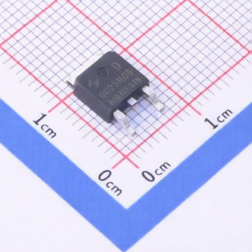
| Drain-to-Source Voltage (VDS) | 1500 | V | |
| Continuous Drain Current (ID) | 3 | A | |
| Continuous Drain Current (ID) at TC = 100 C | 1.7 | A | |
| Pulsed Drain Current (IDM) | 12 | A | Pulse width limited by maximum junction temperature |
| Gate-to-Source Voltage (VGS) | ±30 | V | |
| Single Pulse Avalanche Energy (EAS) | 450 | mJ | IDS=2.5A, VDD=50V, Start TJ=25 |
| Peak Diode Recovery dv/dt | 5.0 | V/ns | ISD =3A,di/dt ≤100A/us,VDD≤BVDS, Start TJ=25 |
| Power Dissipation (PD) - TO-220, TO-3PN, TO-247, TO-263 | 140 | W | |
| Derating Factor above 25C (for TO-220, TO-3PN, TO-247, TO-263) | 1.1 | W/ | |
| Power Dissipation (PD) - TO-220F, TO-3PF | 62.5 | W | |
| Derating Factor above 25C (for TO-220F, TO-3PF) | 0.5 | W/ | |
| Operating Junction and Storage Temperature Range (TJ, Tstg) | -55 to 150 | | |
| Maximum Temperature for Soldering (TL) | 300 | | |
| Junction-to-Case Thermal Resistance (RJC) - No FullPAK | 0.89 | /W | |
| Junction-to-Ambient Thermal Resistance (RJA) - No FullPAK | 62.5 | /W | |
| Junction-to-Case Thermal Resistance (RJC) - FullPAK | 2 | /W | |
| Junction-to-Ambient Thermal Resistance (RJA) - FullPAK | 62.5 | /W | |
| Drain to Source Breakdown Voltage (VDS) | 1500 | V | VGS=0V, ID=250µA |
| Drain to Source Leakage Current (IDSS) at VDS =1500V, VGS= 0V, Tj = 25 | -- | µA | Max: 10 |
| Drain to Source Leakage Current (IDSS) at VDS =1200V, VGS= 0V, Tj = 125 | -- | µA | Max: 500 |
| Gate to Source Forward Leakage (IGSS(F)) at VGS =+30V | -- | nA | Max: 100 |
| Gate to Source Reverse Leakage (IGSS(R)) at VGS =-30V | -- | nA | Max: 100 |
| Drain-to-Source On-Resistance (RDS(ON)) | 5.8 | Ω | VGS=10V, ID=1.5A, Typ. (Max: 8) |
| Gate Threshold Voltage (VGS(TH)) | 3.0 | V | VDS = VGS, ID = 250µA, Min. (Max: 5.0) |
| Gate resistance (Rg) | 3 | Ω | f = 1.0MHz, Typ. |
| Input Capacitance (Ciss) | 1450 | PF | VGS = 0V, VDS = 25V, f = 1.0MHz, Typ. |
| Output Capacitance (Coss) | 87.5 | PF | Typ. |
| Reverse Transfer Capacitance (Crss) | 4.7 | PF | Typ. |
| Turn-on Delay Time (td(ON)) | 25 | ns | ID =1.25A, VDD = 750V, VGS = 10V, RG =5Ω, Typ. |
| Rise Time (tr) | 46 | ns | Typ. |
| Turn-Off Delay Time (td(OFF)) | 45 | ns | Typ. |
| Fall Time (tf) | 60 | ns | Typ. |
| Total Gate Charge (Qg) | 36 | nC | ID =3A, VDD =1000V, VGS = 10V, Typ. |
| Gate to Source Charge (Qgs) | 11 | nC | Typ. |
| Gate to Drain (Miller)Charge (Qgd) | 14 | nC | Typ. |
| Continuous Source Current (Body Diode) (IS) | 3 | A | TC=25 °C |
| Maximum Pulsed Current (Body Diode) (ISM) | 12 | A | |
| Diode Forward Voltage (VSD) | 1.2 | V | IS=3A, VGS=0V, Typ. |
| Reverse Recovery Time (Trr) | 405 | ns | IS=2.5A, Tj = 25°C, dIF/dt=100A/us, VGS=0V, Typ. |
| Reverse Recovery Charge (Qrr) | 2400 | nC | Typ. |
| Reverse Recovery Current (Irrm) | 11.8 | A | Typ. |