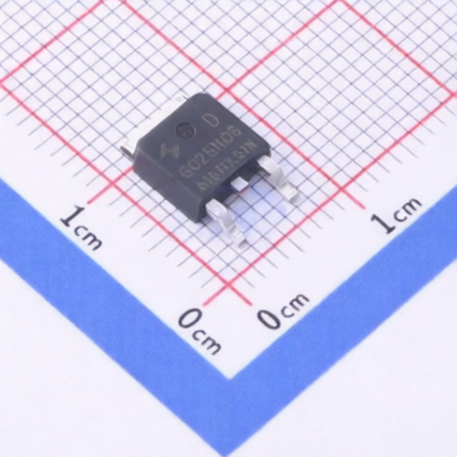
The ASDM30N90Q is a 30V N-Channel MOSFET featuring advanced trench technology and low gate charge. It offers excellent RDS(ON) and high power and current handling capabilities, making it suitable for load switch, PWM applications, and power management scenarios. This MOSFET provides a low gate charge and is designed for efficient power conversion.
| Parameter | Symbol | Conditions | Minimum | Typical | Maximum | Units |
|---|---|---|---|---|---|---|
| Product Summary | ||||||
| Drain-Source Voltage | VDS | 30 | V | |||
| RDS(on), Typ. @ VGS=10V | RDS(on) | VGS=10V | 4.3 | m | ||
| Continuous Drain Current | ID | TC =25C | 90 | A | ||
| Continuous Drain Current | ID | TC =100C | 40 | A | ||
| Absolute Maximum Ratings | ||||||
| Drain-Source Voltage | VDS | (TA =25C unless otherwise noted) | 30 | V | ||
| Gate-Source Voltage | VGS | (TA =25C unless otherwise noted) | 20 | V | ||
| Continuous Drain Current | ID | TC =25C | 90 | A | ||
| Continuous Drain Current | ID | TC =100C | 40 | A | ||
| Pulsed Drain Current | IDM | 360 | A | |||
| Avalanche Current | IS | 90 | A | |||
| Single Pulse Avalanche Energy | EAS | L =0.3mH | 135 | mJ | ||
| Power Dissipation | PD | TC =25C | 65 | W | ||
| Power Dissipation | PD | TC =100C | 32 | W | ||
| Junction and Storage Temperature Range | TJ, TSTG | -55 | 175 | C | ||
| Thermal Characteristics | ||||||
| Maximum Junction-to-Case Steady-State | RJC | 2.3 | C/W | |||
| Maximum Junction-to-Ambient Steady-State | RJA | 62 | C/W | |||
| Electrical Characteristics (TJ =25C unless otherwise noted) | ||||||
| Drain-Source Breakdown Voltage | BVDSS | ID =250A,VGS =0V | 30 | -- | -- | V |
| Zero Gate Voltage Drain Current | IDSS | VDS =30V, VGS =0V, TJ =25C | -- | -- | 1 | A |
| Zero Gate Voltage Drain Current | IDSS | VDS =30V, VGS =0V, TJ =125C | -- | -- | 25 | A |
| Gate-Body Leakage Current | IGSS | VDS =0V, VGS =20V | -- | -- | 100 | nA |
| Gate Threshold Voltage | VGS(th) | VDS =VGS, ID =250A | 1 | 1.6 | 2.4 | V |
| Static Drain-Source On-Resistance | RDS(ON) | VGS =10V, ID =30A | -- | 4.3 | 5.2 | m |
| Static Drain-Source On-Resistance | RDS(ON) | VGS =4.5V, ID =30A | -- | 6.9 | 9.0 | m |
| Forward Transconductance | gFS | VDS =10V, ID =20A | 16 | -- | -- | S |
| Diode Forward Voltage | VSD | IS =30A, VGS =0V | -- | -- | 1 | V |
| Maximum Body-Diode Continuous Current | IS | -- | -- | 90 | A | |
| Dynamic Parameters | ||||||
| Input Capacitance | Ciss | VGS =0V, VDS =15V, f =1MHz | -- | 2120 | -- | pF |
| Output Capacitance | Coss | VGS =0V, VDS =15V, f =1MHz | -- | 307 | -- | pF |
| Reverse Transfer Capacitance | Crss | VGS =0V, VDS =15V, f =1MHz | -- | 253 | -- | pF |
| Switching Parameters | ||||||
| Total Gate Charge | Qg | VGS =10V,VDS =15V, ID =30A | -- | 40 | -- | nC |
| Gate Source Charge | Qgs | VGS =10V,VDS =15V, ID =30A | -- | 5.4 | -- | nC |
| Gate Drain Charge | Qgd | VGS =10V,VDS =15V, ID =30A | -- | 9.6 | -- | nC |
| Turn-On Delay Time | tD(on) | VGS =10V,VDS =15V, ID =20A, RG =3 | -- | 15 | -- | ns |
| Turn-On Rise Time | tr | VGS =10V,VDS =15V, ID =20A, RG =3 | -- | 32 | -- | ns |
| Turn-Off Delay Time | tD(off) | VGS =10V,VDS =15V, ID =20A, RG =3 | -- | 15 | -- | ns |
| Turn-Off Fall Time | tf | VGS =10V,VDS =15V, ID =20A, RG =3 | -- | 12 | -- | ns |
| Body Diode Reverse Recovery Time | trr | IF =30A, di/dt =100A/s | -- | 23 | -- | ns |
| Body Diode Reverse Recovery Charge | Qrr | IF =30A, di/dt =100A/s | -- | 48 | -- | nC |
| Ordering and Marking Information | ||||||
| Device No. | ASDM30N90Q-R | |||||
| Marking | 30N90 | |||||
| Package | DFN5*6-8 | |||||
| Packing Quantity | 4000/Reel | |||||