Apparel & Textile Machinery
(75900)
Building Material Machinery
(55852)
Cleaning Equipment
(104054)
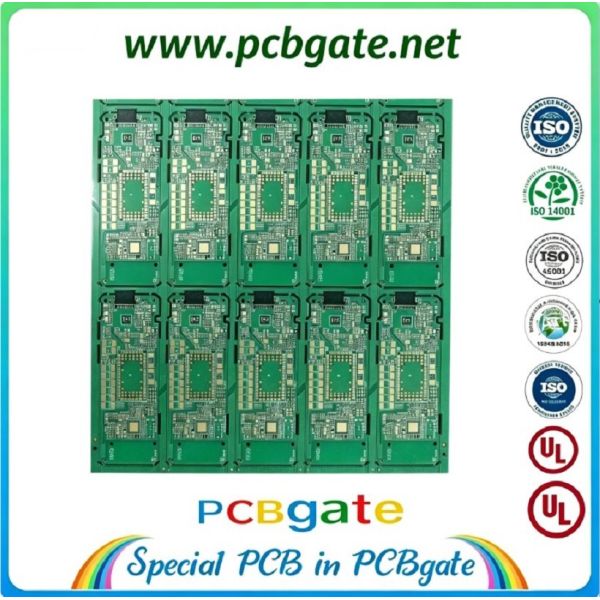
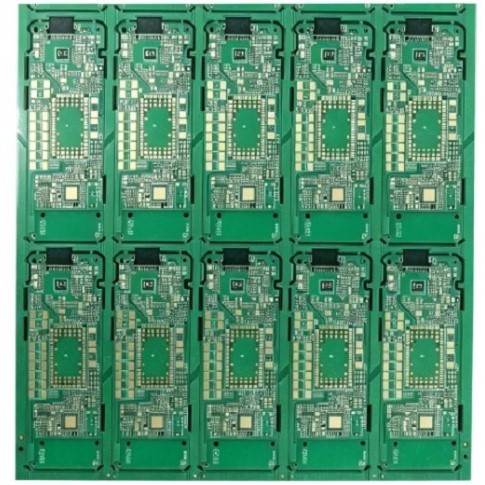
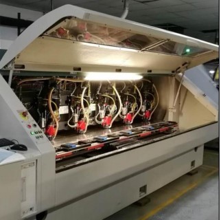
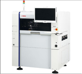
Electronics Production Machinery
(39881)
Energy & Mineral Equipment
(127869)
Engineering & Construction Machinery
(401378)
Environmental Machinery
(35590)
Food & Beverage Machinery
(97353)
Industrial Compressors & Parts
(28499)
Industrial Robots
(3603)
Industry Laser Equipment
(44115)
Machine Tool Equipment
(129643)
Machinery Accessories
(202994)
Machinery Service
(996)
Metal & Metallurgy Machinery
(69132)
Packaging Machine
(102444)
Paper Production Machinery
(29371)

Show all machinery categories
Apparel & Textile Machinery
(75900)
Building Material Machinery
(55852)
Cleaning Equipment
(104054)
Electronics Production Machinery
(39881)
Energy & Mineral Equipment
(127869)
Engineering & Construction Machinery
(401378)
Environmental Machinery
(35590)
Food & Beverage Machinery
(97353)
Industrial Compressors & Parts
(28499)
Industrial Robots
(3603)
Industry Laser Equipment
(44115)
Machine Tool Equipment
(129643)
Machinery Accessories
(202994)
Machinery Service
(996)
Metal & Metallurgy Machinery
(69132)
Packaging Machine
(102444)
Paper Production Machinery
(29371)