Product Description
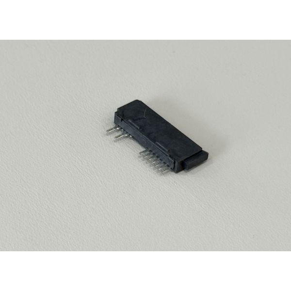
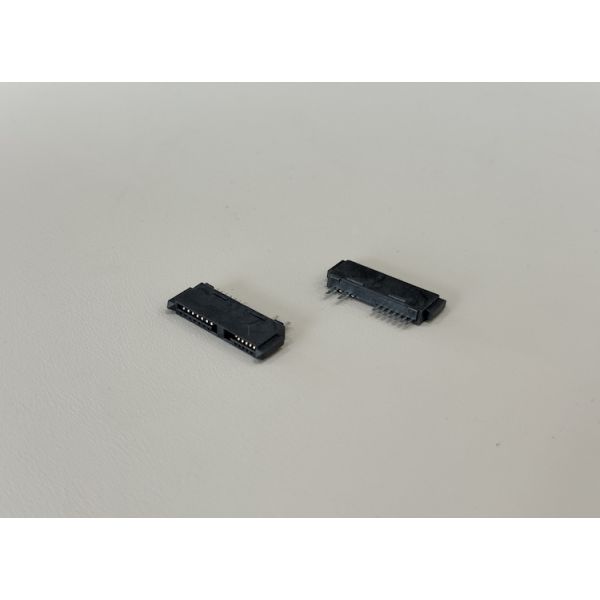
This 13-pin SMT PCB connector is designed for compact electronic equipment where reliable signal and low-power distribution are required on a small footprint. Gold-plated contacts ensure stable transmission and low contact resistance, while the high-temperature, flame-retardant housing supports standard reflow soldering processes.
Reinforced solder tabs on both sides improve PCB retention strength, making the connector suitable for applications exposed to vibration or repeated plugging, such as storage devices, communication equipment, and embedded industrial controllers. Customization of pin count, plating thickness, pitch and keying features is available to match specific harness and mating connector requirements.

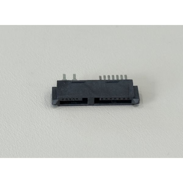
| Connector type | 13-pin SMT PCB signal/power connector |
| Contact pitch | 1.27 mm (custom pitches available) |
| Number of positions | 13 pins |
| Mounting style | Right-angle, surface-mount with hold-down posts |
| Termination to PCB | SMT contacts + soldered retention tabs |
| Contact material | Copper alloy |
| Contact plating | Gold over nickel in mating area, tin on tails |
| Housing material | High-temperature thermoplastic, UL94 V-0 |
| Rated current | Up to 1.5 A per contact (application-dependent) |
| Rated voltage | 30–50 V AC/DC (low-voltage systems) |
| Insulation resistance | ≥ 1000 MΩ @ 500 V DC |
| Contact resistance | ≤ 30 mΩ (initial) |
| Operating temperature | −40 ℃ to +105 ℃ |
| Durability | 500 mating cycles typical |
| Compliance | RoHS / HF / REACH compliant |
Applications
Connection between storage devices (SSD/HDD modules) and main PCBs in computers, set-top boxes and consumer electronics
High-density server and data-center boards, RAID cards, industrial storage backplanes and embedded systems
Communication and networking equipment requiring reliable SATA data and auxiliary power transmission
Customized cable assemblies and adapter boards where a 13-pin SATA style interface is needed
Precautions
Verify that the PCB footprint, pitch and pin assignment match the connector drawing before production.
Do not exceed the specified current and voltage ratings; use appropriate trace width and copper thickness on the PCB.
Maintain correct mating alignment; avoid excessive force, twisting or bending of the connector and solder joints.
Follow recommended reflow or wave-solder profiles for the housing material to prevent deformation.
Keep connectors in a clean, dry environment; avoid contamination of the contact area by flux, dust, oil or moisture.
For harsh environments or special requirements (high mating cycles, thicker gold, special plating), choose customized versions to ensure long-term reliability.