Product Description
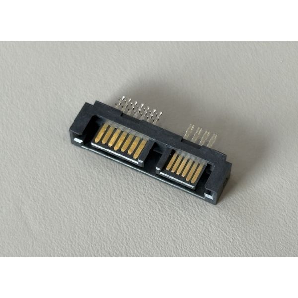
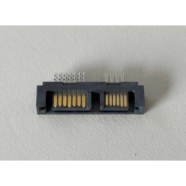
This PCB SATA male connector integrates power and high-speed signal terminals in a compact housing, providing a reliable interface between electronic boards and storage devices. Gold-plated contacts ensure low contact resistance and stable data transmission, while the reinforced housing supports repeated mating cycles in harsh electrical environments. Mixed SMT/through-hole tails improve solder joint strength and alignment on the PCB, making the connector suitable for dense layouts in modern server and industrial boards.
The connector supports customized pin configuration, plating thickness, and special requirements for transmission performance, enabling tailored designs for storage systems, power-signal mixed routing, and OEM cable assemblies.

| Product type | SATA male PCB connector, dual-row power & signal |
| Pin count | 13 pins (combined power/signal design) |
| Mounting style | Right-angle SMT/through-hole mixed tail for PCB |
| Typical pitch | Fine-pitch contacts for compact HDD/SSD interface |
| Contact material | Copper alloy, high conductivity |
| Contact plating | Gold-plated contact area, tin-plated solder tail |
| Housing material | High-temperature thermoplastic, UL94 V-0 |
| Rated voltage | 5–12 V DC (typical SATA power/signal systems) |
| Rated current | Up to 1.5 A per contact (application-dependent) |
| Operating temperature | −40 ℃ to +85 ℃ |
| Insulation resistance | ≥ 1000 MΩ (typical) |
| Withstanding voltage | 500 VAC, 1 minute (typical) |
| Compliance | RoHS / HF / REACH compliant |
| Customization options | Pin length, plating thickness, housing color, packaging |
Applications
Server and data-center storage backplanes, RAID cards, and embedded systems
Industrial control units, PLCs and automation equipment requiring compact SATA interfaces
Automotive infotainment, diagnostic equipment and onboard storage modules
Communication equipment, network appliances and edge-computing devices using SATA drives
Custom PCB-to-device wire and cable assemblies for power and signal transmission
Precautions
Ensure the PCB pad layout strictly follows the connector footprint and pitch to avoid solder bridging and signal integrity issues.
Keep the connector and mating plug free from dust, flux residue and mechanical damage; contamination can increase contact resistance.
Observe recommended reflow or wave-soldering profiles for the high-temperature housing and plated terminals.
Avoid exceeding rated current and voltage on any single pin; distribute power pins evenly for stable operation.
When used in high-speed data paths, follow good PCB design practice (controlled impedance traces, short stubs, solid reference planes) to maintain signal quality.