Specifications
Brand Name :
Phidix
Model Number :
M22001
Certification :
IATF16949,CE
Place of Origin :
China
MOQ :
Negotiable
Price :
Negotiable
Payment Terms :
L/C, D/A, D/P, T/T, Western Union
Supply Ability :
10 PCS/Month
Delivery Time :
40 Work Days
Packaging Details :
1 PC/Wooden Box
Color :
White
Customization :
OEM, ODM
Packing :
1 PC/Carton
Warranty :
1 year
Lead-time :
40 Work Days
Resolution :
15nm, 20nm
Magnification :
60,000X
Accelerating Voltage :
5kV to 30kV
Signal Detection :
(SEI)-Secondary Electron Image
Electron Gun :
Filament type, Pre Centered tungsten filament Cartridge
Max Sample size :
70mm in diameter, 30mm in height
Image format :
BMP, JPEG, PNG,TIFF
Vacuum system :
High Vacuum Mode
Description

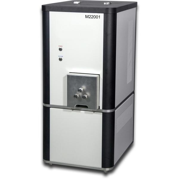
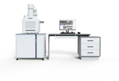
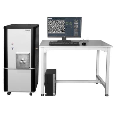
Magnification Max 60,000X Scanning Electron Microscope 15nm Resolution with Optional EDS

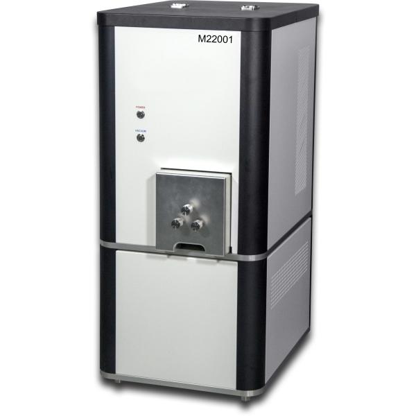
As the basic desktop SEM, M22001 series can meet the basic experimental needs of most users. It is equipped with SE (secondary electron) detector and BSE (backscattered electron) detector. The load platform can be configured with three axes (X, Y, R). The manual platform can also be upgraded to a five-axis (X, Y, R, Z, T) automatic platform. The EDS spectrum analyzer can be configured in all series of products. The products include the following configurations:

Specials:

- Magnification Max 60,000X.

- Signal Detection: SE Detector+BSE Detector.

- Accelerating Voltage:5kV to 30KV, High image resolution.

- EDS is optional, for component analysis.

- High Vacuum System.

- Tilt Stage configuration (0~45°)( optional).

Item Specification M22001
Resolution 15nm (30kV, SE Image) ●
20nm (30kV, BSE Image) ●
Magnification 30x~60,000x ●
Accelerating Voltage 5kV to 30kV (5kV/10kV/15kV/20kV/30kV-5 step) ●

Signal Detection

(SEI)-Secondary Electron Image ●
(BSEI)-Backscattered Electron Image ○
* Multi Detector (SEI+BSEI) ○
Observation mode Standard Mode ●
Charge-up reduction mode ●
Electron Gun Filament type, Pre Centered tungsten filament Cartridge ●
Bias voltage system, Automatic mode ●
Electron gun alignment, Manual mode ●
Lens system Focus Lens, 2-stage Electromagnetic Condenser Lens ●
Objective Lens, 1-stage Electromagnetic Objective Lens ●
Detector type, SE Detector/ BSE Detector ●
Stage system

Auto or Manual

Stage Traverse, 3 axis system, X, Y-axis : 35mm / R-axis: 360°

●
Image shift Image shift X, Y Image Shift (±150um) ●
Max sample size 70mm in diameter, 30mm in height ●
Image scanning system Fast Scan: 320x240 (Scan time: 0.1 sec.) ●
Slow Scan: 640x480 (Scan time: 3 sec.) ●
Photo Mode 1: 1280x960 ●
Photo Mode 2: 2560x1920 ●
Photo Mode 3: 5120x3840 ●
Image format BMP, JPEG, PNG,TIFF ●
Data display Magnification, Detector type, Accelerating Voltage, Vacuum mode, Logo(Text), Date and time, Text marker, scale bar ●
Vacuum system

Fully Automatic Multi mode, High vacuum

Rotary Pump/100Liters/min

Turbo Molecular Pump/ 70Liters/sec

pump down time: less than 3 minutes

●
Control unit system

Mouse, Keyboard

PC

●
Software function

Image file open, edit, Save function

Length, area, angle measuring

parameter initialization, mage capture mode conversion), Archives, Setting(EDS)

●
Volume Main Unit-460(W)×600(D)× 950(H)mm……1set
External vacuum pump-400(W)×160(D)×340(H)mm …1set
●
Weight 99kg ●
Equipment environment

Temperature: 15℃~30℃
Humidity: 70% or less

Power source: Single phase 200~240V AC, 1KW, 50/60Hz

●

Accessories package:

Pre Centered tungsten filament 5 pcs/box ●

Sample Stage

15mm dia. (10 pcs) ●
25mm dia. (10 pcs) ●
15mm 45° Tilt (5 pcs) ●
15mm 90° Tilt (5pcs) ●
Height standard master 1ea ●
allen wrench 1set ●
SEM Software CD 1ea ●
Carbon conductive tape 1roll ●
scissors 1ea ●
tweezers 1ea ●
Tools Box 1ea ●

Note: ● means standard, ○ means optional

The sample test results

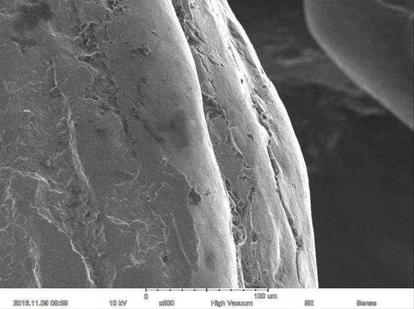
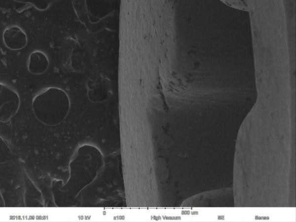
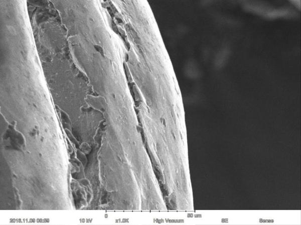
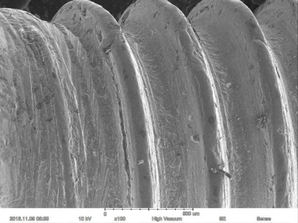
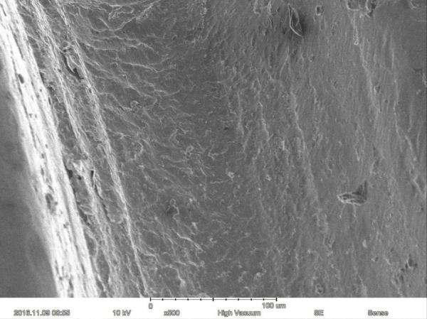
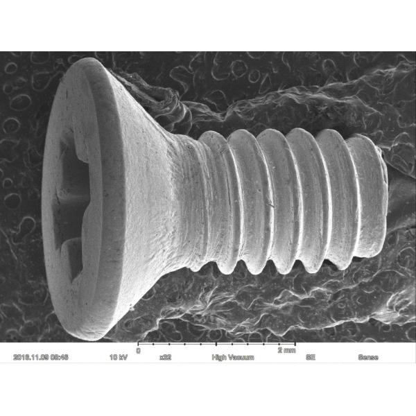
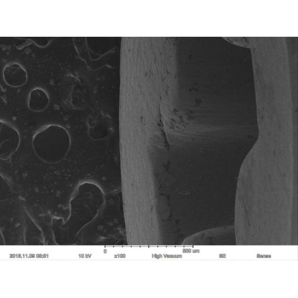
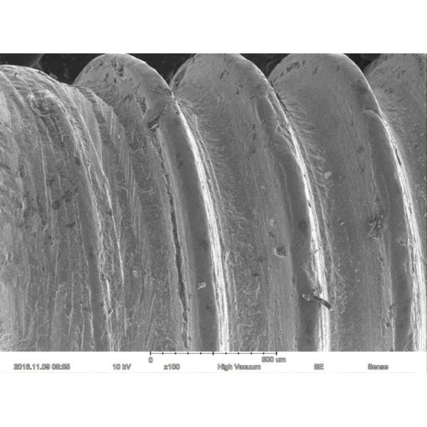
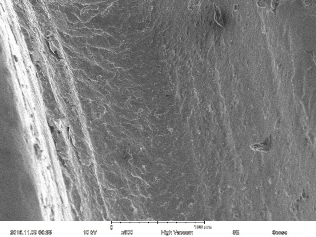
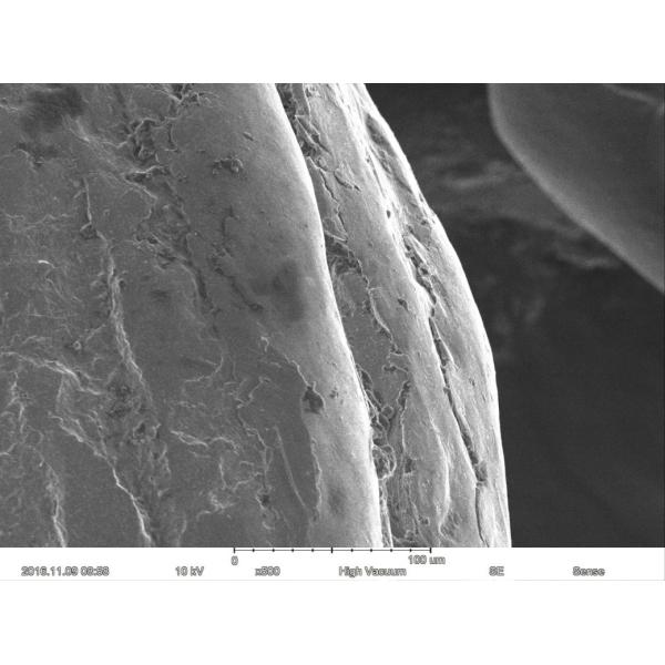
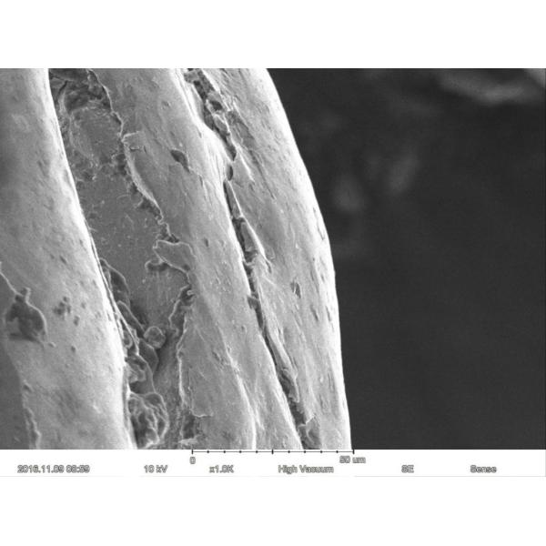
We conducted a practical test using a defective screw that was discarded in the laboratory as a sample. The pictures are as follows:

Magnification Max 60000X Scanning Electron Microscope 15nm Resolution Optional EDS

Screw, ×47, 30 kV, SE, High Vacuum

Magnification Max 60000X Scanning Electron Microscope 15nm Resolution Optional EDS

×100, 10kV, SE, High Vacuum

Magnification Max 60000X Scanning Electron Microscope 15nm Resolution Optional EDS

×100, 10kV, SE, High Vacuum

Magnification Max 60000X Scanning Electron Microscope 15nm Resolution Optional EDS

×500, 10kV, SE, High Vacuum

Magnification Max 60000X Scanning Electron Microscope 15nm Resolution Optional EDS

×500, 10kV, SE, High Vacuum

Magnification Max 60000X Scanning Electron Microscope 15nm Resolution Optional EDS

×1000, 10kV, SE, High Vacuum

Other Pictures:

Magnification Max 60000X Scanning Electron Microscope 15nm Resolution Optional EDS

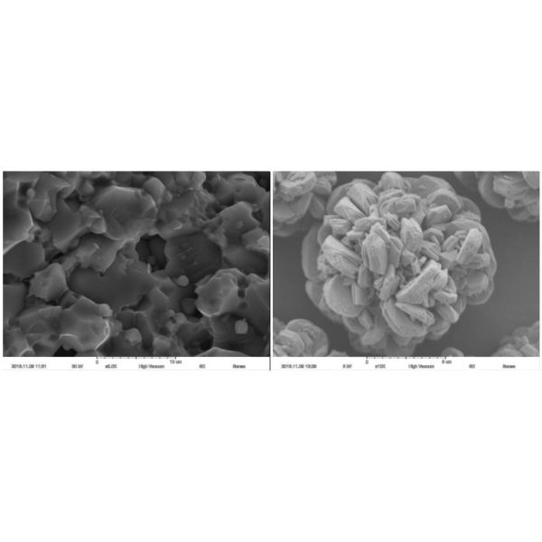
Ceramic ×5000 Battery material ×10K

Magnification Max 60000X Scanning Electron Microscope 15nm Resolution Optional EDS

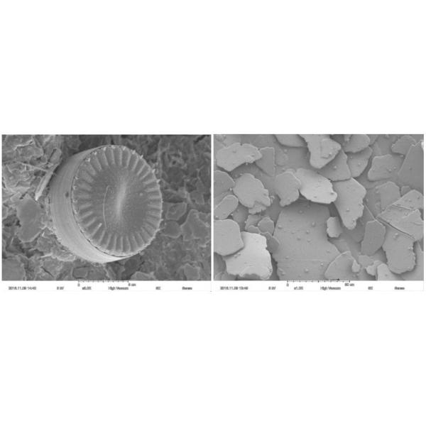
Phytoplankton ×8000 Pearl powder ×1000

Magnification Max 60000X Scanning Electron Microscope 15nm Resolution Optional EDS

Send your message to this supplier
Send Now

Magnification Max 60000X Scanning Electron Microscope 15nm Resolution Optional EDS

Ask Latest Price
Brand Name :
Phidix
Model Number :
M22001
Certification :
IATF16949,CE
Place of Origin :
China
MOQ :
Negotiable
Price :
Negotiable
Contact Supplier
Magnification Max 60000X Scanning Electron Microscope 15nm Resolution Optional EDS

Phidix Motion Controls (Shanghai) Co., Ltd.

Active Member
6 Years
shanghai, shanghai
Since 2004
Business Type :
Manufacturer, Exporter
Employee Number :
100~120
Certification Level :
Active Member
Contact Supplier
Submit Requirement