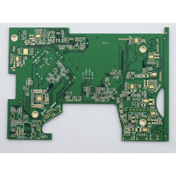
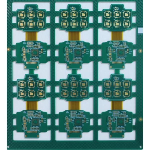
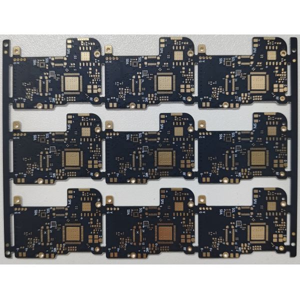
Compact Custom HDI PCB for Mini PC - High Integration & Space-Saving Design
Advantages of HDI Circuit Boards
An HDI PCB (High Density Interconnect Printed Circuit Board) is a specialized type of circuit board that has a higher wiring density per unit area compared to conventional PCBs. It uses advanced technologies like microvias, blind and buried vias, and fine lines and spaces to pack more components and connections into a smaller footprint.
Benefits of Custom HDI PCBs
Choosing a custom PCB means you get exactly what your project needs, not a generic design that compromises on performance. Off-the-shelf boards are built for mass markets, so they often include unnecessary features while lacking the specific connections, power delivery, or layout you require.
With a custom PCB, you can optimize the layout for shorter signal paths, better cooling, and improved stability—critical for high-speed CPUs, GPUs, and memory. You also gain full control over component selection, allowing you to prioritize quality, cost, or specific technologies.
Production Process Flow
- Design and Engineering Preparation - The client provides design files (such as Gerber files), and the engineering team conducts Design for Manufacturability (DFM) analysis, optimizing the layout to ensure microvia and trace accuracy, while selecting appropriate substrate materials (such as FR-4 or high-frequency laminates).
- Inner Layer Fabrication and Drilling - Fabricating inner-layer circuits on the substrate: Copper layers are etched to form circuits via photolithography, followed by laser drilling (or mechanical drilling) to create microvias (typically with diameters less than 0.15mm) for high-density interconnections.
- Pore Metallization and Lamination - Chemically plate the holes with copper or fill them with conductive materials to make the hole walls conductive; then laminate all inner and outer layers together under high temperature and pressure to ensure precise alignment of each layer.
- Outer Layer Manufacturing and Surface Treatment - Add outer layer circuit: After graphic transfer and etching, perform surface treatment (such as gold immersion, OSP, or silver immersion) to enhance solderability and oxidation resistance.
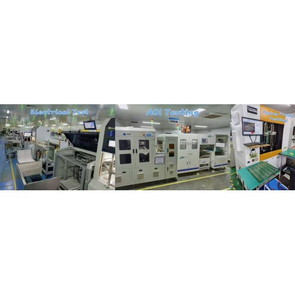
- Testing and Final Processing - Conduct rigorous circuit function testing (including AOI and electrical testing), confirm defect-free results, then proceed with trimming, cleaning, and packaging for shipment.
Quality Assurance & Certifications
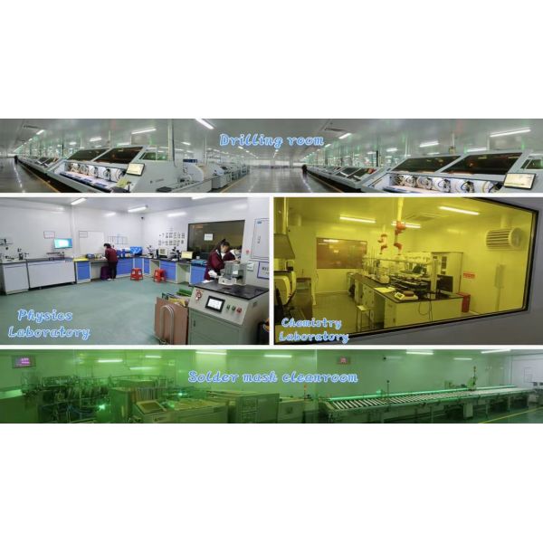
Factory Showcase
PCB Quality Testing
Advanced Inspection Equipment
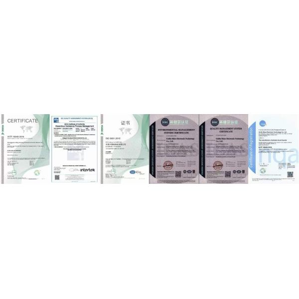
Certificates and Honors