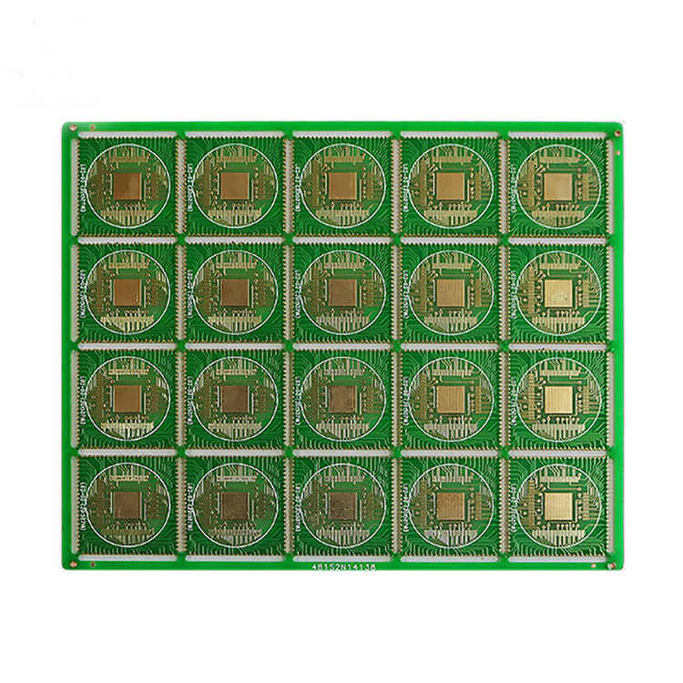
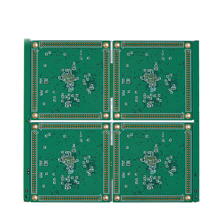
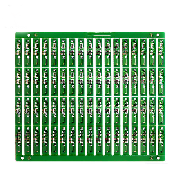
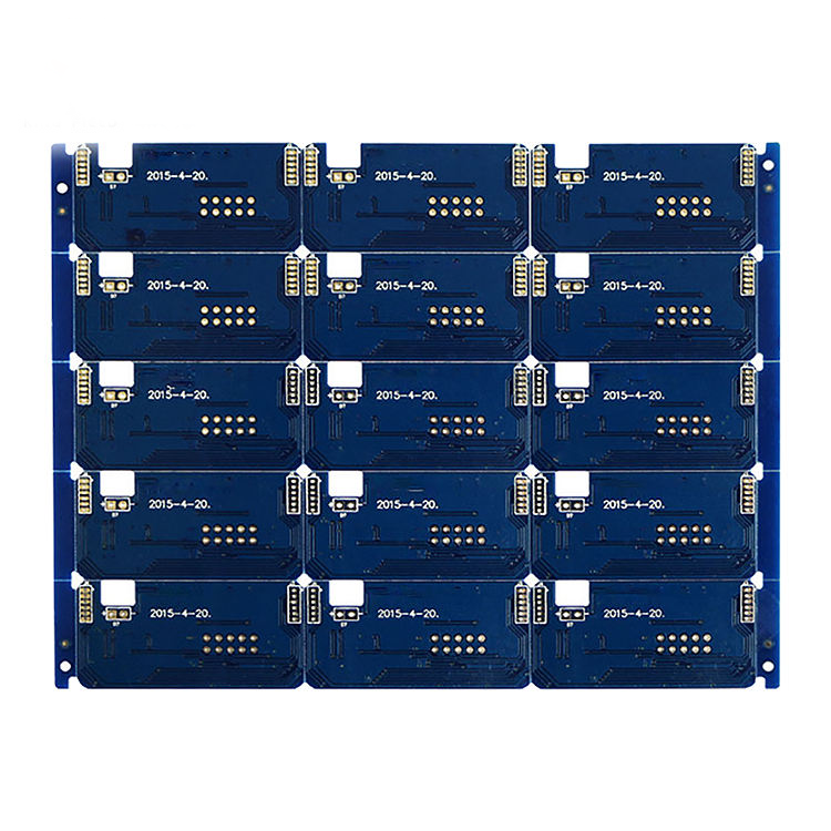
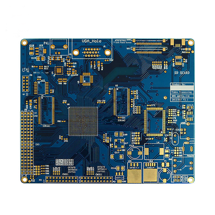
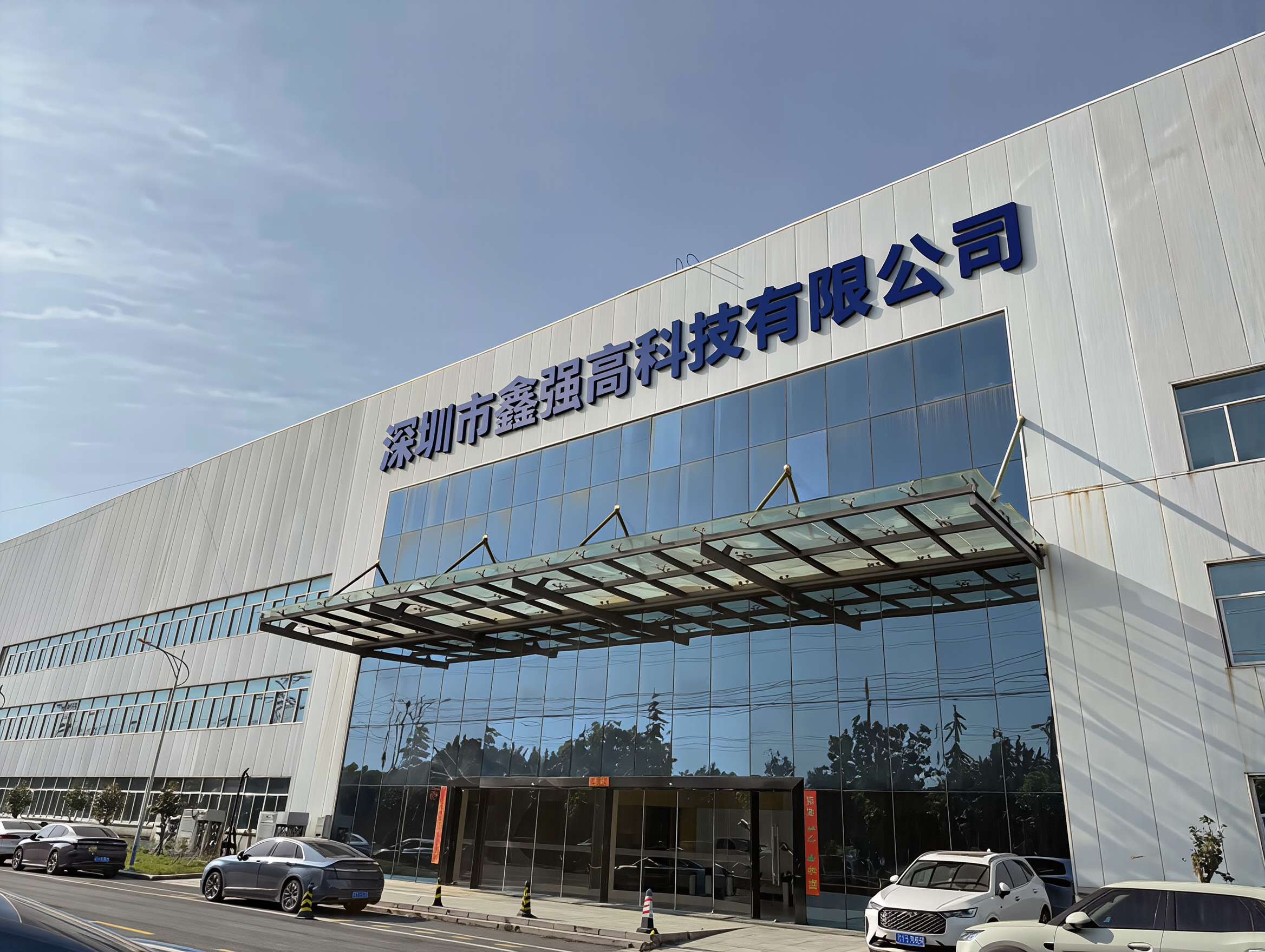
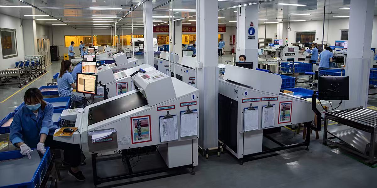
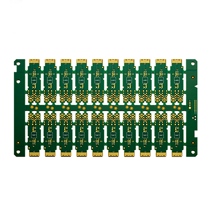
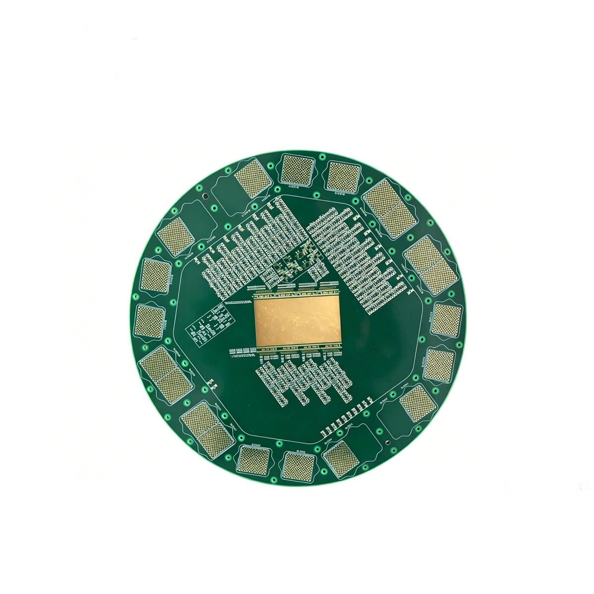
Shenzhen Hing Technology Co., Ltd was established in 2016. The company is a national high-tech enterprise specializing in the research and development, production and sales of printed circuit boards. Since its establishment, the company has long adhered to the development strategy of quality first, technology as the core, and customer demand as the orientation, focusing on the high-end segmented circuit board market covering an area of approximately 10000 square meters.
The company's products are widely used in communication, new energy, industrial control, consumer electronics, automotive electronics and medical electronics and other application fields, and the products serve well-known customers at home and abroad.
| o. | Capabilities | Standard Production | Advanced Production | ||
|---|---|---|---|---|---|
| 1 | Stack up | Blind/Buried/Anylayer board | Lamination times | MAX≤5times | MAX≤6times |
| Copper thickness | Inner layer | 1/3OZ-2oz MAX 2OZ |
1/4OZ-2oz MAX OZ |
||
| Outer layer | 1/3OZ-3OZ | 1/3OZ-2OZ | |||
| Min Dielectric ThK | 35um(1027) | 30um (1017) | |||
| Structure | 1-N-1 / 2-N-2 / 3-N-3 | 1-N-1 / 2-N-2 / 3-N-3 / 4-N-4 / ELIC(12L) | |||
| Layer count | 4-24 | 4-34 | |||
| 2 | Min. Line/Space | Min L/W (inner) | 2/2mil (50/50um) | 1.6/1.6 mil ( 40/40um) | |
| Min. L/W (Outer) | 2.4/2.4mil (60/60um) | 2/2mil (50/50um) | |||
| 3 | Line/Space | Inner Layer | Tenting | 2/2mil (50/50um) | 1.6/1.6 mil ( 40/40um) |
| mSAP | 1.4/1.4mil (40/40um) | 1.2/1.2mil (35/35um) | |||
| Outer layer | Tenting | 3/3mil (75/75um) | 2.4/2.4 mil ( 60/60um) | ||
| mSAP | 2.4/2.4mil (60/60um) | 2/2mil (50/50um) | |||
| Pad size | inner layer min size | 225um | 200um | ||
| outter layer min size | 225um | 200um | |||
| 4 | Drill | min Mechanical Drill size | 0.2mm | 0.15mm | |
| PTH plating A/R | ≤8:1 | ≤10:1 | |||
| PTH Hole Tolerance | ±0.075mm | ±0.075mm | |||
| NPTH Hole Tolerance | ±0.05mm | ±0.05mm | |||
| Plated slot tolerance | Long slot | ±0.075mm | ±0.075mm | ||
| Short Slot | ±0.1mm | ±0.1mm | |||
| 5 | Min BGA | Min BGA/ BGA pitch | 0.4 | 0.35 | |
| 6 | Laser | Min. Laser hole size | 75um | 50um | |
| Min. distance from laser hole to laser hole | 0.025mm | 0.025mm | |||
| Laser hole plating A/R | ≤0.8:1 | ≤1:1 | |||
| 7 | Soldermask | Color | Green,Yellow,Black,Blue,Red, White, Matt green | Green,Yellow,Black,Blue,Red, White, Matt green | |
| SM ThK | Single print thickness | 10-30um | 10-30um | ||
| Min SM dam | 3.0mil | 2.5mil | |||
| 8 | Impedance | Capability of Impedance | Single line impedance<50Ω | ±3.5Ω | ±3.5Ω |
| Single line impedance≥50Ω | ±10% | ±7% | |||
| Differential line impedance | ±10% | ±7% | |||
| 9 | Tolerance capability | Patten size tolerance | pad size tolerance | ±20% | ±15% |
| line tolerance | ±20% | ±15% | |||
| patten to outline | +/- 0.0075mm | +/- 0.0050mm | |||
| Registration tolerance | laser A/R | 100um | 75um | ||
| PTH A/R | 100um | 75um | |||