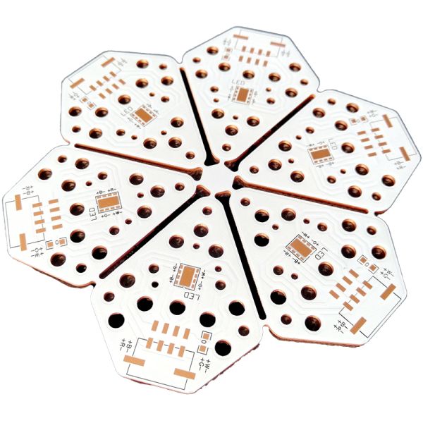
When a single-layer aluminum PCB runs out of routing room, the answer is our double-layer aluminum PCB. Two copper layers are separated by an insulating prepreg and laminated onto an aluminum base; plated through holes (PTH) electrically connect the top and bottom circuit layers, while the aluminum core continues to do what FR4 cannot — pull heat out of the board and spread it across a large, low-resistance metal mass.
In this structure, the bottom copper layer sits against the thermal dielectric and aluminum base, so power devices and LEDs are typically placed on the bottom side for the shortest heat path, while control, logic, and connector circuitry occupies the top layer. Through holes can also be engineered as thermal vias under components to pass heat into the base. Where a design requires both circuit layers on the same side of the aluminum, or bottom-side components with drilled, insulated aluminum, we review the design in DFM and propose the most manufacturable stackup.
Compared with an FR4 4-layer board plus external heat sink, a double-layer aluminum PCB often delivers the same function in a thinner, lighter, cheaper assembly — one board that routes the signals, carries the current, and cools the components. All boards are produced under ISO 9001, ISO 13485, and IATF 16949 quality systems and are RoHS compliant and UL certified.
| Layer count | 2 copper layers on aluminum base (other MCPCB structures on request) |
|---|---|
| Board structure | Cu L1 → prepreg/FR core → Cu L2 → thermal dielectric → aluminum base |
| Copper thickness | 1 – 3 oz (35 – 105 µm) per layer |
| Aluminum base thickness | 1.0 / 1.5 / 2.0 / 3.0 mm |
| Total board thickness | 1.2 – 2.5 mm (typical 1.6 mm) |
| Thermal conductivity (dielectric) | 1.0 – 3.0 W/m·K |
| Dielectric breakdown voltage | ≥ 2 kV AC |
| Min trace width / spacing | 0.15 mm / 0.15 mm |
| Min finished PTH size | 0.5 mm (via filling/plugging available) |
| Max panel size | 600 × 500 mm |
| Surface finish | ENIG, HASL (LF), OSP, Immersion Silver/Tin |
| Solder mask / silkscreen | White, Green, Black, Blue / White, Black |
| Board outline | CNC routing, punching, V-scoring |
| Testing | 100% electrical test (flying probe / fixture); impedance control available |
| Prototype lead time | 7 – 9 working days; mass production 12 – 18 working days |
A: A double-sided FR4 board has copper on both sides of an insulating core with no metal base — heat stays trapped in the board and needs an external heat sink. A double-layer aluminum PCB adds a thermally conductive dielectric and an aluminum base, so heat flows directly into the metal core. You get similar routing density with dramatically better thermal performance.
A: In the standard stackup, the bottom copper layer is closest to the thermal dielectric and aluminum base, so power devices and LEDs belong on the bottom layer for the shortest heat path; the top layer carries control and logic. Our engineers review this during DFM and confirm the best arrangement for your design.
A: The aluminum base is conductive, so standard vias stop at the circuit stack. Insulated, drilled-through-aluminum structures are possible as a special process — send your files and we will confirm feasibility, cost, and lead time.
A: Yes. Vias under thermal pads can be plated and plugged (filled with epoxy and capped with copper) to conduct heat from the top layer down to the aluminum base — a standard option on our 2-layer MCPCB.
A: It costs more due to lamination, drilling, and plating, but it is often cheaper in total than a 4-layer FR4 board with a separate heat sink, insulation pad, and assembly hardware. Cost depends on hole count, size, and copper weight — send Gerbers for a detailed quote.
A: Prototypes in 7–9 working days, mass production in 12–18 working days, slightly longer than single-layer aluminum due to the lamination and PTH processes.
A: Yes. Controlled-impedance fabrication is available; share your impedance requirements and we will confirm the stackup and coupon testing.
A: Yes — SMT and through-hole assembly on both layers, component sourcing, and functional/burn-in testing, delivered as finished modules.