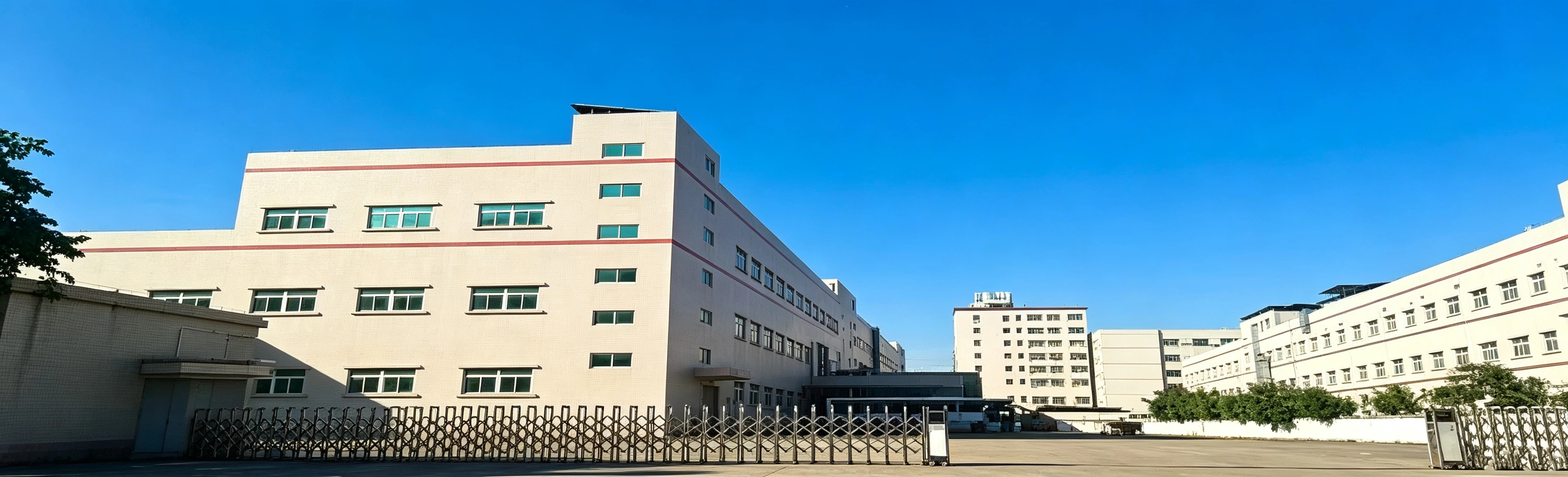
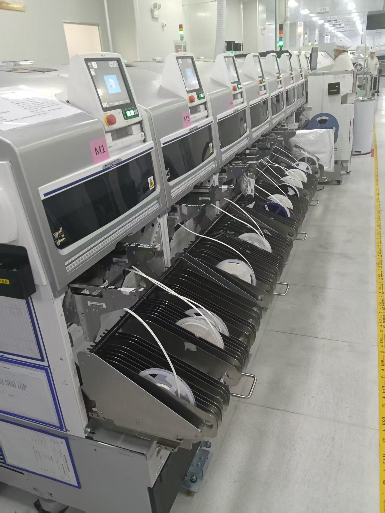
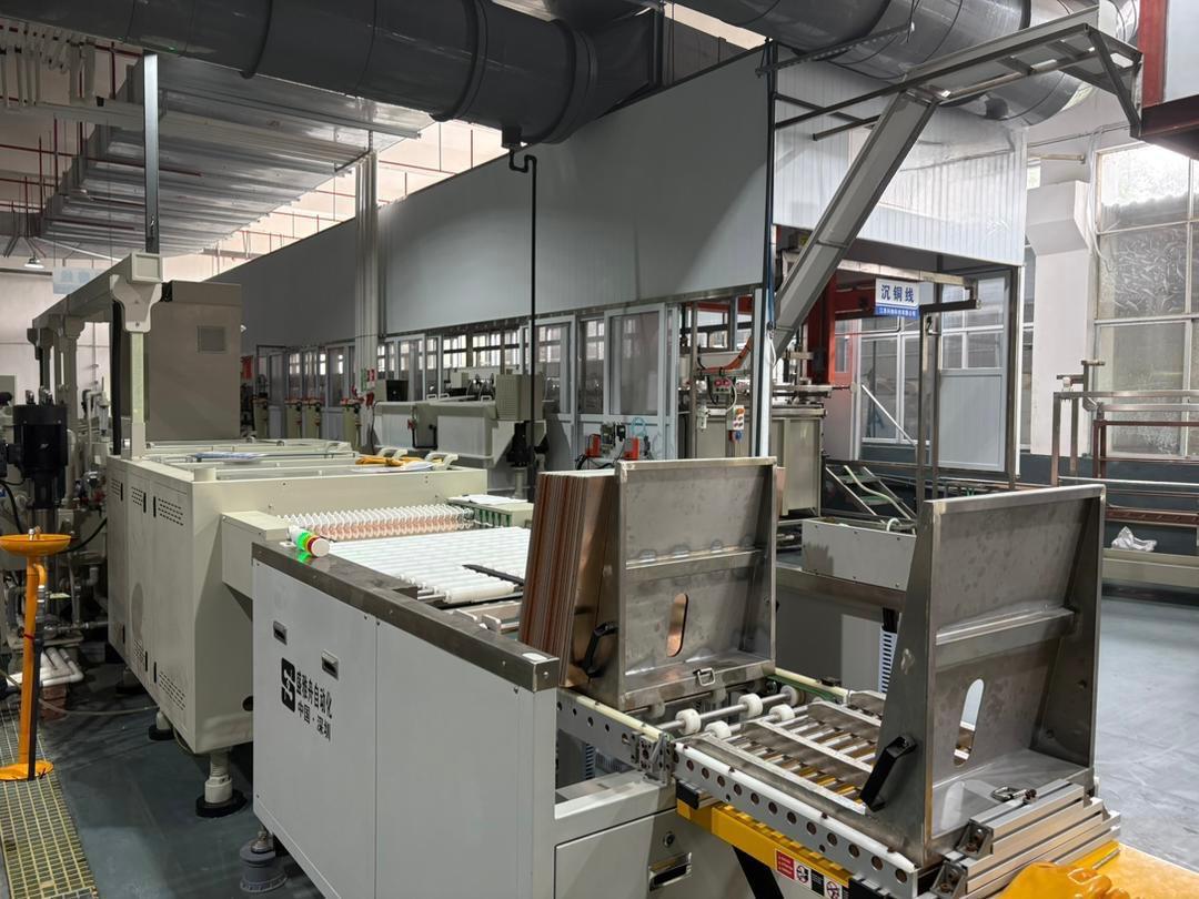
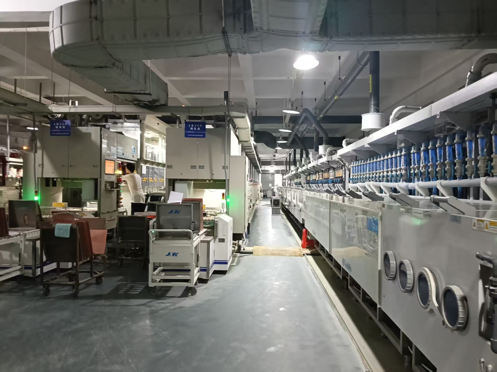
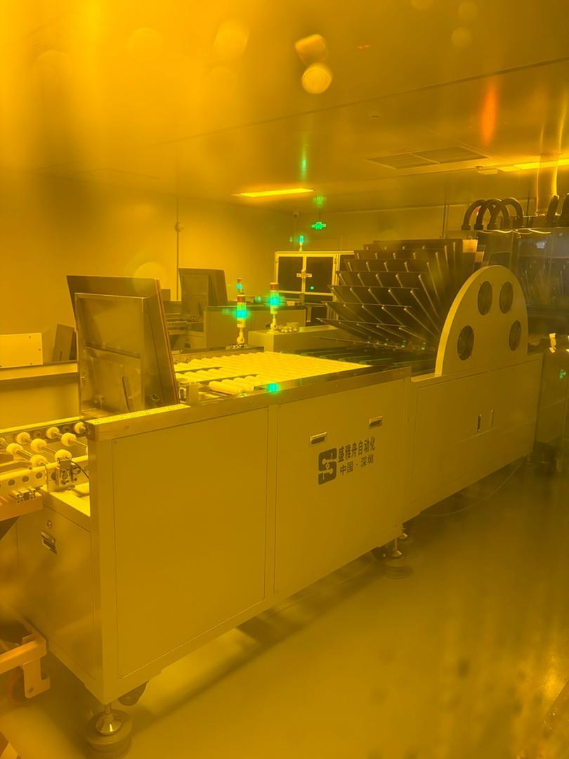
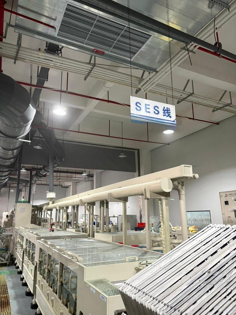
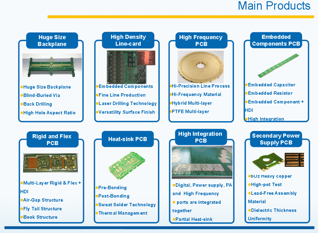
Jiaqing Circuit was founded in 2012 in Shenzhen, China. We own a 5,000 square meter manufacturing plant with a monthly PCB production capacity of 20,000 square meters, capable of manufacturing 2-48 layer PCBs.
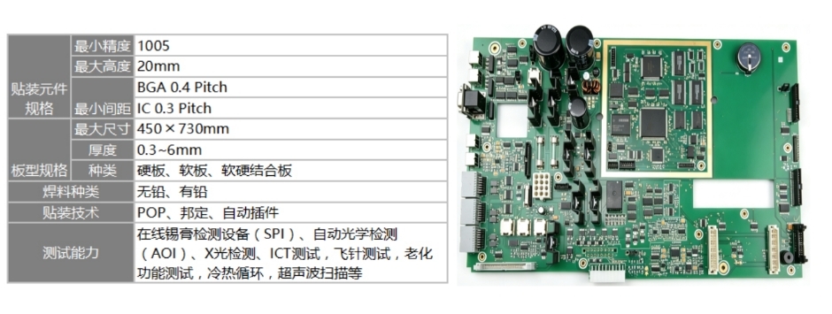
We deliver one-stop solutions including PCB design, PCB fabrication, BOM component sourcing and SMT assembly. Our products serve high-end industries such as automotive electronics, industrial control, AI computing, telecommunications and medical electronics.
With mature manufacturing processes and stable supply-chain support, we handle rapid prototyping, small-batch and mass-production orders. We strive to provide reliable custom-printed circuit board solutions for global high-tech electronics customers.


JQPCB has a dedicated engineering and R&D team focused on pushing PCB manufacturing boundaries. We work closely with customers from design to mass production, helping turn complex electronic designs into reliable, manufacturable boards.
Our engineers speak fluent technical English and are experienced in customer drawings and international standards. From prototype review to mass production, we stand behind every board we ship.
Send us your Gerber files and specifications, and our engineering team will support your project from day one.
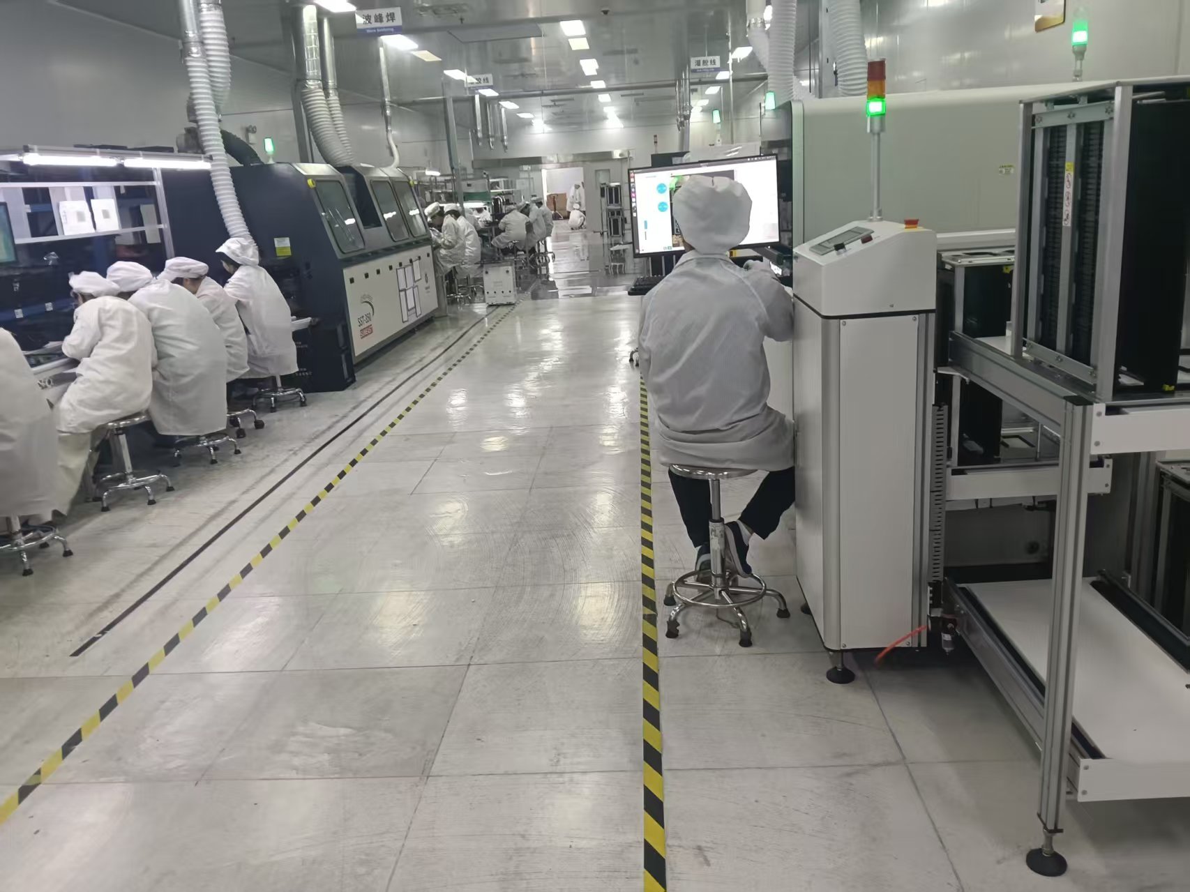
JQPCB is supported by an experienced and dedicated team covering engineering, production, quality control and customer service. Our people are the foundation of the quality and reliability we deliver to every customer.
We believe a reliable PCB supplier is more than equipment — it is the people behind the process. Our team works closely together to understand each customer's requirements and deliver boards that meet specifications on time.
When you work with JQPCB, you work with a team that speaks your technical language and takes responsibility for your project.
JQPCB was founded with a simple mission: to be a reliable and professional PCB manufacturing partner for engineers and companies worldwide.
From our early days, we focused on building solid foundations in quality, process control and on-time delivery. What started as a standard PCB fabrication workshop has grown into a specialized manufacturer serving demanding industries.
Today, JQPCB combines stable manufacturing capability, strong engineering support and competitive pricing. We continue to invest in equipment and process improvement to support our customers' most challenging projects.
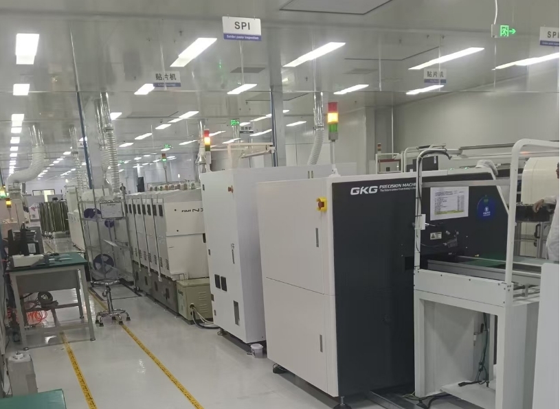
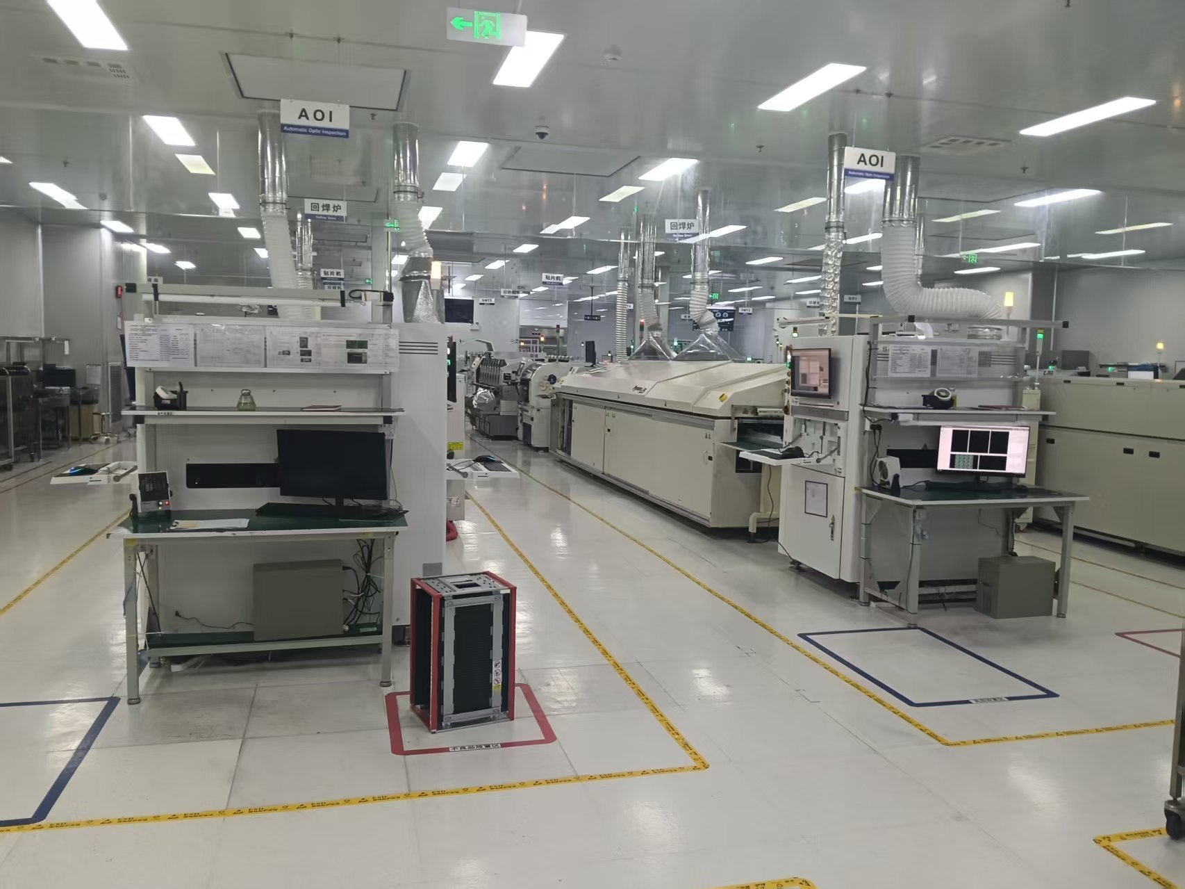
We are committed to providing one-stop, full‑process electronic manufacturing services covering four core areas: BOM sourcing, CAD design, PCB fabrication, and SMT assembly. In BOM sourcing, we offer professional component selection and supply chain procurement to ensure material quality and on‑time delivery. Our CAD design capabilities handle complex, high‑density, and high‑speed board designs, supporting up to 48 layers, 40,000 pins, and 28 Gbps differential signaling, meeting the most demanding requirements. Our PCB fabrication utilizes advanced precision processing, supporting minimum trace width/spacing of 2 mil, minimum mechanical drilled hole of 6 mil, and laser microvia of 4 mil, to satisfy high‑reliability product needs. Our SMT assembly is equipped with state‑of‑the‑art placement lines, enabling high‑accuracy surface‑mount and assembly. By integrating the entire chain from material procurement and design development to production assembly, we help customers effectively shorten R&D cycles, reduce overall costs, and enhance the market competitiveness of their final products.
| Parameter | Specification |
|---|---|
| Maximum number of layers | 48 layers |
| Maximum pin count | 40,000 |
| Maximum connection points (nets) | 20,000 |
| Minimum mechanical drilled hole | 6 mil |
| Minimum laser via (microvia) | 4 mil |
| Minimum trace width / spacing | 2 mil / 2 mil |
| Maximum number of BGAs per board | 15 |
| Minimum BGA pad pitch | 15 mil |
| Maximum BGA pin count per device | 2,400 |
| High‑speed differential signaling | 28 Gbps, and 14 Gbps up to 40 inches |
| Design methodology | Constraint‑driven design (rule‑driven design) |