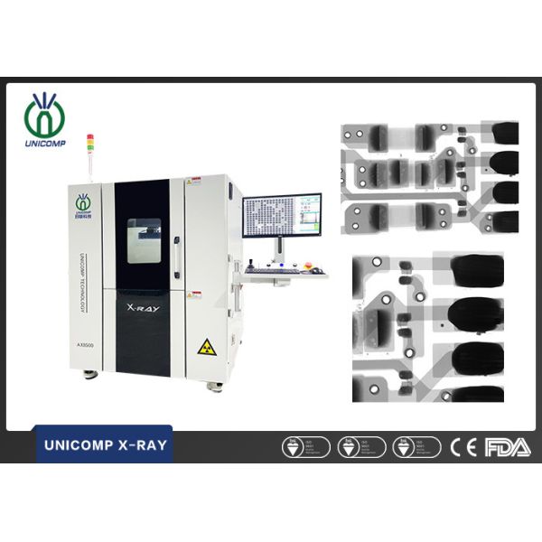
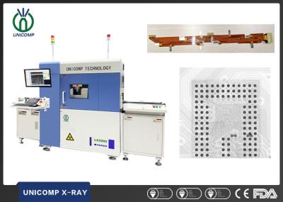
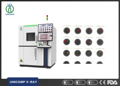
160KV Microfocus X-ray Inspection Machine for Semiconductor Wire Bonding NDT AX9600 Unicomp
The UNICOMP AX9600 160KV microfocus X-ray inspection system is equipped with a proprietary 160kV high-power open-type microfocus X-ray tube, achieving an ultra-fine focal spot of merely 0.8 μm. Supporting a maximum geometric magnification of 2000× with superior X-ray penetrability, this system enables precise void fraction quantification for TVS diodes and serves as a high-accuracy inspection solution tailored for advanced IC packaging, HBM storage dies, and GPU semiconductor device quality verification.
Technical Specifications
System Summary
| Dimensions |
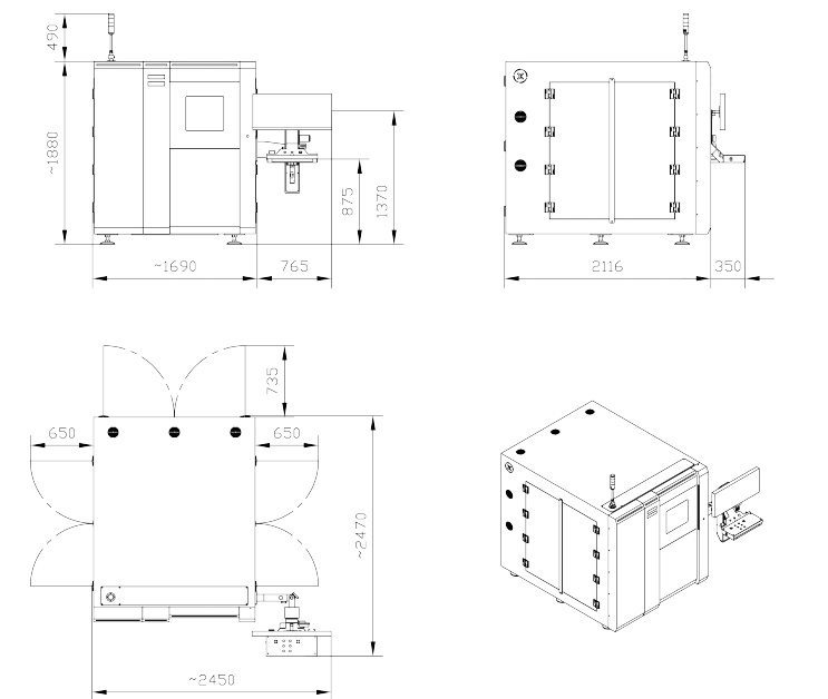
1690mm(L)×2116mm(W)×1880mm(H) |
| Weight |
4590kg |
| Power Supply |
220V±10% 50Hz/60Hz 9A |
| Power Consumption |
2kw |
X-ray Tube
| Tube Type |
Open Type |
| Voltage |
160kv |
| Max. Power |
64W |
| Min.Resolution |
1µm |
Imaging System
| X-ray Detector |
FPD |
| Pixel Size |
84µm |
| Detection Area |
129*129mm |
| Pixel Matrix |
1536*1536[pixel] |
| Frame Rates |
Max 30fps |
| System Magnification |
34000X |
Motion Control System
| Max. Payload Size |
520*520[mm] |
| Max. Detection Size |
520*520[mm] |
| X/Y/Z-Axis Travel Distance |
550/710/265[mm] |
| Tilt and Rotation |
Detect XY±70° Tilt |
Industrial PC
| Motion Control Mode |
34"HD 4K curved display |
| Operating System |
Windows 11 64-bit |
| Storage |
4TB HDD+512G SSD |
| Memory |
32G |
| Processor |
i5 12 generation |
Other Features
| Door Operation |
Automatic Door |
| X-Ray Safety |
<1µSv/h |
Applications
The UNICOMP AX9600 high-power microfocus X-ray inspection system is engineered for ultra-precision non-destructive evaluation (NDE) of advanced semiconductors and microelectronic components. It delivers high-fidelity void fraction quantification for TVS diodes, alongside internal flaw inspection for advanced IC packages, HBM high-bandwidth memory dies, GPU modules and high-density electronic assemblies.
Extensively deployed for quality validation across automotive electronics, power semiconductors, aerospace-grade electronic hardware and miniature precision components, the system facilitates precise characterization of micro-voids, solder joint anomalies, internal fractures and assembly irregularities. It provides robust technical backing for R&D validation and mass production process quality control within the high-end semiconductor manufacturing sector.
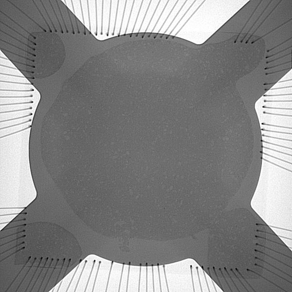
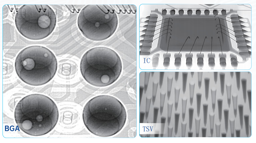
Inspection Images
Sample Inspection Image
System Dimensions and Appearance