Product Overview
3C-SiC, also known as Cubic Silicon Carbide or β-SiC, is an important polytype of silicon carbide. Unlike the commonly used 4H-SiC and 6H-SiC, 3C-SiC has a cubic crystal structure and offers excellent semiconductor, thermal, mechanical and chemical properties.
3C-SiC features a wide bandgap, high thermal conductivity, high mechanical strength, good chemical stability and promising electronic properties. It is widely used in MEMS, sensors, power device research, optoelectronic devices, photonics, epitaxial research and high-temperature applications.
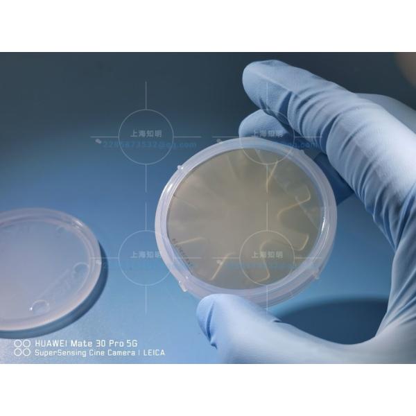
Common 3C-SiC products include 3C-SiC substrates, 3C-SiC on Si wafers, 3C-SiC thin films and customized epitaxial structures. Among them, 3C-SiC on Si is widely used in research and development because it combines the material advantages of 3C-SiC with the cost and process compatibility of silicon substrates.

Material Features
Cubic Crystal Structure
3C-SiC is the cubic polytype of silicon carbide. Its crystal structure is different from the hexagonal structures of 4H-SiC and 6H-SiC. Due to this special structure, 3C-SiC has unique advantages in epitaxial growth, interface properties, electronic performance and device research.
Good Electronic Properties
3C-SiC has promising electronic properties and is considered suitable for high-speed electronic devices, high-frequency devices and power device research.
Excellent Thermal Performance
3C-SiC has good thermal conductivity and can be used in applications requiring high thermal stability and efficient heat dissipation, such as power devices, RF devices, optoelectronic devices and high-temperature sensors.
High Chemical Stability
3C-SiC has good resistance to corrosion, oxidation and harsh chemical environments. It is suitable for harsh-environment sensors, high-temperature MEMS devices and special industrial applications.
Good Mechanical Strength
3C-SiC has high hardness, high mechanical strength and good wear resistance. It can be used for micro-mechanical structures, pressure sensors, resonators, cantilever structures and thin-film mechanical devices.
Compatible with Silicon-Based Processes
3C-SiC can be grown on silicon substrates to form 3C-SiC on Si wafers. This structure helps reduce cost and improves compatibility with mature silicon-based semiconductor processes, making it attractive for MEMS, sensors and CMOS-compatible research.
Product Types
3C-SiC Substrate
3C-SiC substrates are suitable for material research, power device development, epitaxial growth, thermal management and new wide-bandgap semiconductor device research.
Available options include:
- N-type 3C-SiC substrate
- High-resistivity 3C-SiC substrate
- Semi-insulating 3C-SiC substrate
- Single-side polished 3C-SiC wafer
- Double-side polished 3C-SiC wafer
- Customized size, thickness, orientation and resistivity
3C-SiC on Si Wafer
3C-SiC on Si refers to a 3C-SiC film grown on a silicon substrate. This product combines the cost advantage of Si substrates with the excellent properties of 3C-SiC, and is suitable for MEMS, sensors, thin-film devices and silicon-based integration research.
Common structures include:
- 3C-SiC / Si
- 3C-SiC / SiO₂ / Si
- 3C-SiC thin film on Si substrate
- Customized buffer layer structure
- Customized epitaxial thickness structure
3C-SiC Thin Film
3C-SiC thin films can be used for micro/nano fabrication, etching research, sensor structures, photonic platforms, waveguide devices and thin-film mechanical testing.
Different thicknesses, orientations, surface roughness levels and substrate structures can be customized according to customer requirements.
Customized Epitaxial Structure
Customized 3C-SiC epitaxial structures can be provided according to customer R&D requirements, including different substrates, film thicknesses, doping types, resistivity ranges and surface processing requirements.
Typical Specifications
| Item |
Available Options |
| Material |
3C-SiC / β-SiC / Cubic SiC |
| Crystal Structure |
Cubic |
| Product Type |
3C-SiC substrate, 3C-SiC on Si, 3C-SiC thin film, customized epi wafer |
| Wafer Size |
2 inch, 4 inch, 6 inch or customized |
| Orientation |
<100>, <111> or customized |
| Conductivity Type |
N-type, high-resistivity, semi-insulating or customized |
| Substrate Material |
Si, SiC or other customized substrates |
| Epitaxial Thickness |
Customized according to requirements |
| Wafer Thickness |
Customized according to drawings or specifications |
| Surface Treatment |
SSP / DSP |
| Surface Roughness |
Controlled according to customer requirements |
| Testing Items |
Thickness, resistivity, TTV, bow, warp, surface defects, orientation, etc. |
| Packaging |
Single wafer box, wafer cassette, vacuum packaging, clean packaging |
Product Advantages
Suitable for High-Temperature Applications
3C-SiC has good high-temperature stability and is suitable for high-temperature sensors, high-temperature MEMS, engine monitoring, industrial control, aerospace applications and harsh-environment detection.
Suitable for MEMS Devices
Due to its high mechanical strength, good thermal stability and corrosion resistance, 3C-SiC is an important material for high-temperature MEMS and harsh-environment MEMS. It can be used for pressure sensors, gas sensors, resonators, cantilever structures and micro-mechanical films.
Suitable for Silicon-Based Integration Research
3C-SiC on Si can be combined with silicon-based processing technology, making it suitable for universities, research institutes and enterprise R&D departments working on SiC and Si process integration.
Suitable for Optoelectronic and Photonic Devices
3C-SiC can be used in optoelectronic devices, integrated photonic platforms, UV detectors, waveguide structures and new semiconductor optical devices.
Suitable for Power Semiconductor Research
As a wide-bandgap semiconductor material, 3C-SiC offers high breakdown field strength, high thermal stability and good electronic properties. It is suitable for research on new power devices, MOS structures and device reliability.
Supports Customized Requirements
We can provide customized 3C-SiC products according to customer requirements, including wafer size, thickness, orientation, conductivity type, epitaxial structure and surface processing standards.
Main Applications
MEMS Devices
- High-temperature MEMS
- Pressure sensors
- Gas sensors
- Acceleration sensors
- Resonators
- Cantilever structures
- Micro-mechanical thin-film structures


Optoelectronic and Photonic Devices
- UV detectors
- LED research
- Optical waveguides
- Integrated photonic platforms
- Quantum photonic devices
- Photonic crystal structures
Sensor Applications
- High-temperature pressure sensors
- Corrosive gas sensors
- Industrial environment sensors
- Aerospace sensors
- Automotive electronic sensors
- Energy equipment monitoring sensors
Epitaxy and Material Research
- SiC epitaxial growth research
- 3C-SiC defect research
- Lattice mismatch research
- Thin-film stress research
- Heteroepitaxial structure research
- Wide-bandgap material research
Difference Between 3C-SiC, 4H-SiC and 6H-SiC
4H-SiC and 6H-SiC are common silicon carbide polytypes, and 4H-SiC is widely used in commercial power devices. In comparison, 3C-SiC has a cubic crystal structure and shows unique advantages in electron mobility, silicon-based epitaxial growth, MEMS devices, sensors and thin-film device research.
In simple terms:
- 4H-SiC is more commonly used for mature power devices;
- 6H-SiC is used in some optoelectronic, substrate and special applications;
- 3C-SiC is more suitable for MEMS, Si-based epitaxy, sensors, thin-film devices, photonic devices and new power device research.
Therefore, 3C-SiC is not simply a replacement for 4H-SiC. The selection depends on the device structure, process route and research purpose.
FAQ
1. What is 3C-SiC?
3C-SiC, also known as cubic silicon carbide or β-SiC, is a polytype of silicon carbide with a cubic crystal structure. It offers excellent thermal stability, chemical resistance, mechanical strength and semiconductor properties.
2. What is the difference between 3C-SiC and 4H-SiC?
3C-SiC has a cubic crystal structure, while 4H-SiC has a hexagonal crystal structure. 4H-SiC is widely used in commercial power devices, while 3C-SiC is commonly used for MEMS, sensors, Si-based epitaxy, thin-film devices, photonics and material research.
3. What types of 3C-SiC products can you provide?
We can provide 3C-SiC substrates, 3C-SiC on Si wafers, 3C-SiC thin films and customized 3C-SiC epitaxial structures according to customer requirements.
About Us
ZMSH specializes in high-tech development, production, and sales of special optical glass and new crystal materials. Our products serve optical electronics, consumer electronics.We offer Sapphire optical components, mobile phone lens covers, Ceramics, LT, Silicon Carbide SIC, Quartz, and semiconductor crystal wafers. With skilled expertise and cutting-edge equipment, we excel in non-standard product processing, aiming to be a leading optoelectronic materials high-tech enterprise.

Packaging & Shipping Information
Packaging Method:
- All items are securely packed to ensure safe transit.
- Packaging features anti-static, shock-resistant, and dust-proof materials.
- For sensitive components such as wafers or optical parts, we adopt cleanroom-level packaging:
- Class 100 or Class 1000 dust protection, depending on product sensitivity.
- Customized packaging options are available for special requirements.
Shipping Channels & Estimated Delivery Time:
- We work with trusted international logistics providers, including:
UPS, FedEx, DHL
- Standard lead time is 3–7 business days depending on the destination.
- Tracking information will be provided once the order is dispatched.
- Expedited shipping and insurance options are available upon request.