Specifications
Delivery Time :
5-15 Working days
Surface Finish :
ENIG / HASL / OSP
Material :
FR4 PCB substrate
OperatingTemperature :
-40°C to 85°C
Board Thickness :
0.4 – 3.2 mm
AssemblyTechnology :
SMT and DIP
Packaging Details :
Vacuum Package+Carton Box
Supply Ability :
Double Sided: 12000 sq m / month Multilayers: 8000sq.m / month
Operating Frequency :
Up to 6 GHz
Power SupplyVoltage :
3.3V, 5V, or 12V
SurfaceFinish :
ENIG (Electroless Nickel Immersion Gold)
Operating Temperature :
-40°C - 85°C
Insulation Resistance :
≥1000MΩ
Payment Terms :
T/T,Western Union,Paypal
Application :
Communication devices and systems
Price :
Negotiable
Testing :
AOI, X-ray, functional testing
Compliance Standards :
RoHS, IPC-A-610 Class 2
Layers :
1~64 layers
Solder Mask Color :
Green (customizable)
Compliance :
RoHS, REACH
Function :
Signal processing and transmission
ImpedanceControl :
50 Ohm controlled impedance
SignalIntegrity :
High, with impedance matching and shielding
Model Number :
PCBA for Communication
Certification :
ISO9001, TS16949, UL, RoHS
Brand Name :
Support OEM / ODM
Pcb Layers :
2 – 20+layers
Dimensions :
Customizable based on design
Component Type :
SMD and through-hole components
Place of Origin :
China
MOQ :
1-10 pcs
Type :
Communication device PCBA
Description

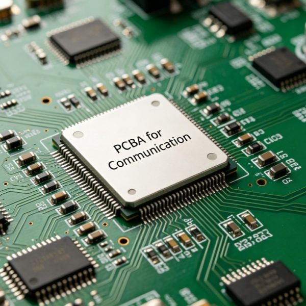
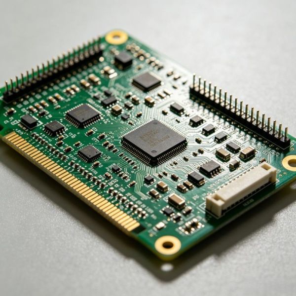
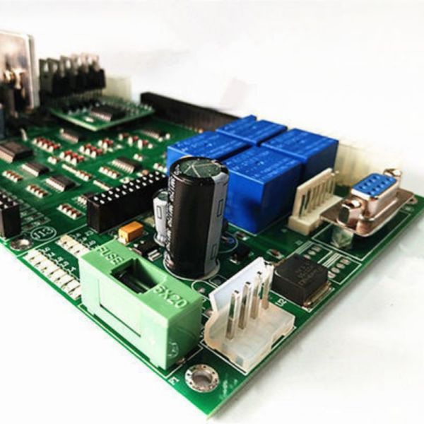
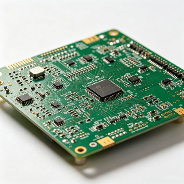
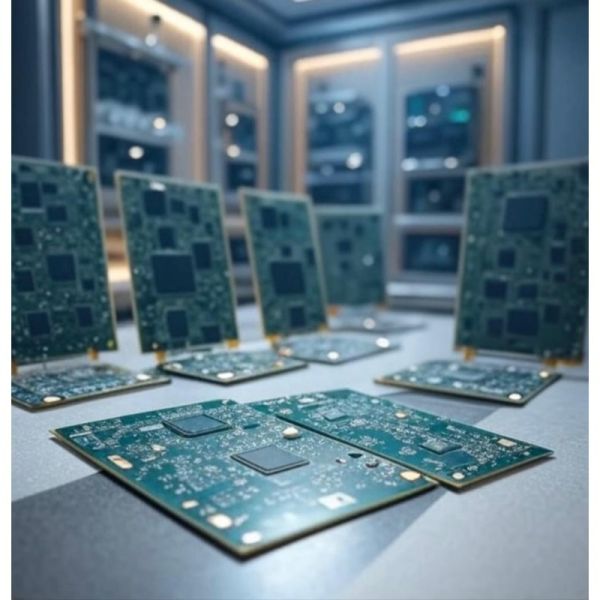
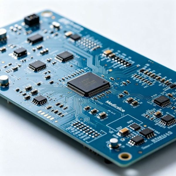
Our PCBA for Communication solutions is engineered to meet the demanding requirements of modern telecom and networking systems. From 5G infrastructure to data transmission equipment, we provide high-performance, stable, and scalable PCB assembly services tailored for communication applications.

With strict quality control and advanced manufacturing capabilities, we ensure every board delivers signal integrity, reliability, and long-term performance.

Applications in the Communication Industry

Our communication PCBA solutions are widely used in:

  • 5G / 4G Base Stations
  • Optical Fiber Communication Equipment
  • Network Switches & Routers
  • RF & Microwave Systems
  • IoT Communication Modules
  • Satellite Communication Devices
  • Data Centers & Server Boards

Key Advantages

1. High Signal Integrity

  • Controlled impedance design
  • Low-loss materials (Rogers, Taconic, etc.)
  • Optimized stack-up for high-frequency applications

2. Precision Manufacturing

  • Support for HDI & multilayer PCB (up to 40+ layers)
  • Fine pitch components (BGA, QFN, 0201/01005)
  • Advanced SMT & DIP assembly lines

3. Reliability for Harsh Environments

  • Wide operating temperature range
  • Anti-interference design (EMI/EMC optimization)
  • Conformal coating & protection options

4. Fast Turnaround & Flexible Production

  • Prototype (24–72 hours)
  • Small batch to mass production
  • Agile supply chain for urgent telecom projects

5. Strict Quality Control

  • 100% AOI / X-ray inspection
  • ICT / Functional Testing
  • IPC Class 2 / Class 3 standards
  • ISO9001 / ISO13485 compliant

Our PCBA Capabilities

Item Capability
PCB Layers 1–40 Layers
Min Line Width/Spacing 3/3 mil
Assembly Type SMT, THT, Mixed
Component Size 01005
BGA Pitch 0.3mm
Testing AOI, X-ray, ICT, FCT
Lead Time 24H Prototype

Why Choose Us for Communication PCBA?

  • Experience in telecom & networking projects
  • Strong component sourcing ability (especially IC shortages)
  • DFM/DFA support to reduce risk and cost
  • One-stop service: PCB + Components + Assembly + Testing
  • Dedicated project manager (提高信任感,促进转化)

Challenges We Help You Overcome

  • Signal instability in high-frequency boards
  • Delays due to component shortages
  • Poor soldering quality on fine-pitch ICs
  • Lack of reliable suppliers for telecom-grade PCBA

We provide stable, tested, and telecom-grade solutions to eliminate these risks.

From Prototype to Mass Production

We support your project at every stage:

  1. Engineering Review (DFM Check)
  2. PCB Fabrication
  3. Component Sourcing
  4. SMT Assembly
  5. Testing & Quality Assurance
  6. Global Delivery

Start Your Communication PCBA Project Today

  • Send your Gerber files & BOM
  • Get a fast quotation within 12 hours
  • Free engineering consultation

Get Instant Quote Now
Talk to an Engineer

Send your message to this supplier
Send Now

FR4 AOI Testing PCBA for Communication Telecom Networking PCB Assembly 0.4-3.2mm

Ask Latest Price
Delivery Time :
5-15 Working days
Surface Finish :
ENIG / HASL / OSP
Material :
FR4 PCB substrate
OperatingTemperature :
-40°C to 85°C
Board Thickness :
0.4 – 3.2 mm
AssemblyTechnology :
SMT and DIP
Contact Supplier
FR4 AOI Testing PCBA for Communication Telecom Networking PCB Assembly 0.4-3.2mm

Guangdong Jiefu Technology Co., Ltd.

Verified Supplier
1 Years
guangdong, shenzhen
Since 2010
Business Type :
Trading Company, Exporter
Total Annual :
6,600,000-9,000,000
Employee Number :
100~150
Certification Level :
Verified Supplier
Contact Supplier
Submit Requirement