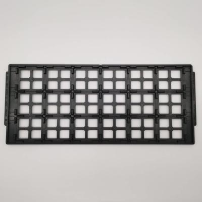
JEDEC IC Trays Protect Wafers From Contamination And Damage In Production Handling
Looking for reliable protection for delicate semiconductor wafers during production handling? PC JEDEC IC Tray shields wafers from contamination and physical harm, built with durable PC material to withstand frequent industrial use.
Need seamless compatibility with automated production lines? PC JEDEC IC Tray follows strict JEDEC standards, reducing wafer failure rates and supporting consistent quality control across all manufacturing stages.
Want tailored solutions for diverse wafer sizes? PC JEDEC IC Tray offers customizable cavities, delivering reliable, contamination-free protection for sensitive semiconductor wafers in high-volume production or precision handling scenarios.
Key Features/ Benefits
- Durable PC material construction
- Contamination and dust control
- Safeguard wafer packaging processes
- RoHS compliant materials
- Flexible customization
Specifications
| Brand |
Hiner-pack |
| Model |
HN25065 |
| Material |
PC |
| Package Type |
JEDEC |
| Color |
Black |
| Resistance |
1.0×10⁴ - 1.0×10¹¹ Ω |
| Outline Line Size |
322.6×135.9×12.19 mm |
| Cavity Size |
52×50×4.31 mm |
| Matrix QTY |
2X5=10 PCS |
| Warpage |
MAX 0.74mm |
| Service |
Accept OEM, ODM |
| Custom Pocket Options |
Available |
Applications
PC JEDEC IC Tray serves semiconductor wafer production lines, clean room manufacturing, and industrial handling. It blocks dust and particle contamination, preserving wafer purity during high-precision production.
PC JEDEC IC Tray also supports in-process handling and storage, offering stable protection between production steps. Custom cavities hold wafers firmly, minimizing shifting and impact during automated operations.
Customized Services
Offer end-to-end customization for JEDEC IC trays. Collaborate with engineering teams to define cavity pitch, pocket depth, and material properties for specific wafer sizes and thicknesses. Develop anti-static or high-temperature resistant variants, and validate prototypes through in-house testing. Deliver fully tailored tray solutions that optimize production flow and minimize contamination risks for advanced semiconductor manufacturing.
About Us:
Hiner-pack® was founded in 2013. It is a high-tech enterprise that integrates Design, R&D, Manufacturing, Sales of IC packaging and testing, as well as semiconductive wafer fabrication process in automated handling, carrying, and transportation to provide customers with turnkey services.
Why Choose Us:
- Rich experience in JEDEC / IC / Waffle Pack Trays
- In-house mold design capability
- Fast prototype development
- Strict QC process
- Stable supply for global semiconductor customers