Specifications
Thickness :
0.02mm - 1.5mm
Tolerance :
+/- 0.005mm
Materials :
Brass, Brass Alloy, Cooper, Copper Alloy
Production Process :
Photo Chemical Etching, Plating, Stamping, Laser cutting
Brand Name :
XHS/ Customized
Model Number :
Custom
Certification :
ISO 9001, ISO 14001
Place of Origin :
China
MOQ :
10
Price :
50-100USD
Payment Terms :
T/T
Supply Ability :
10000-100000PCS / week
Delivery Time :
3-15 days
Packaging Details :
PE bags and Cartons / Customized
Description

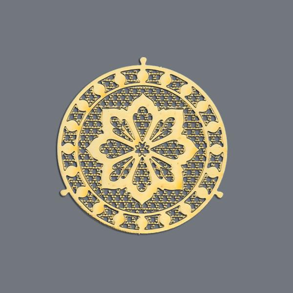
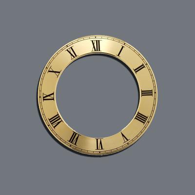
Photo Chemical Etching High Precision Copper Lead Frames For Electronics

Xinhaisen - 13 years ISO-certified photochemical etching expert
Specializes in semiconductor lead frames & precision metal components. Processes metal materials (stainless steel/copper/titanium) with ±0.01mm tolerance.

Specifications of Copper Lead Frame:
Material Copper, Brass Alloys etc.
Brass Alloys +/-0.005mm
Shape Customized
Applications Semiconductor IC packaging
Technique Chemical etching, Plating, Stamping, Laser cutting
Feature No burrs, no broken point and clean
Project Case of Copper Lead Frames for reference:
Photo Chemical Etching High Precision Copper Lead Frames For Electronics Photo Chemical Etching High Precision Copper Lead Frames For Electronics
Applications of Copper Lead Frames:
  • Semiconductor Packaging: Essential in the assembly of microchips and semiconductors, providing an efficient electrical connection between components.

  • Microelectronics: Used in microelectronic devices, such as MEMS (Micro-Electromechanical Systems), for precise integration of electrical components.

  • LED Lighting: Supports LED components, ensuring the electrical leads are positioned correctly for optimal performance and longevity.

  • Automotive Electronics: Key components in automotive circuit boards and electronic systems that require reliable, high-precision lead frames.

  • Telecommunications: Used in the manufacturing of telecommunications equipment, ensuring durable and efficient connections.

Photo Chemical Etching High Precision Copper Lead Frames For Electronics
Features of Photo Chemical Etching:
  • High Precision: The photo chemical etching process allows for extremely detailed and accurate patterns, ensuring that every lead frame meets the exact specifications required for your application.

  • Durable Copper Material: Copper’s excellent electrical conductivity and corrosion resistance make it the ideal choice for lead frames, ensuring long-term performance even in demanding environments.

  • Customizable Design: Lead frames can be customized according to your exact specifications, providing flexibility in design and meeting your specific product requirements.

  • Cost-Effective Manufacturing: Photo chemical etching is a cost-effective process for creating intricate shapes and features without the need for expensive molds or tooling.

  • High Quality: Our copper lead frames are made with the highest standards of quality control to guarantee reliable performance and consistent results.

How to etching lead frame from us?

1.Please send us your design.
We accept the following file formats: DWG, DXF, PDF, Step, Gerber, IGES, CorelDraw and AI.

2.Samples making lead time:3-10days

3.Express:By DHL,Fedex,TNT,around 3-7days.

Send your message to this supplier
Send Now

Photo Chemical Etching High Precision Copper Lead Frames For Electronics

Ask Latest Price
Watch Video
Thickness :
0.02mm - 1.5mm
Tolerance :
+/- 0.005mm
Materials :
Brass, Brass Alloy, Cooper, Copper Alloy
Production Process :
Photo Chemical Etching, Plating, Stamping, Laser cutting
Brand Name :
XHS/ Customized
Model Number :
Custom
Contact Supplier
video
Photo Chemical Etching High Precision Copper Lead Frames For Electronics

Shenzhen Xinhaisen Technology Limited

Verified Supplier
2 Years
guangdong, shenzhen
Since 2012
Business Type :
Manufacturer, Exporter
Total Annual :
4000000-6000000
Employee Number :
260~300
Certification Level :
Verified Supplier
Contact Supplier
Submit Requirement