Specifications
Certification :
ISO9001
Delivery Time :
10 work days
Payment Terms :
T/T
Customized Services :
Materials, specifications, precision, etc. can be customized
Supply Ability :
The average monthly production capacity for calibration plates and film is 300,000 pieces
Shipping Option :
FedEx And UPS
Packaging Details :
Cardboard boxes or plastic boxes packaging
Place of Origin :
China
MOQ :
10
Brand Name :
DFOPTIX
Description

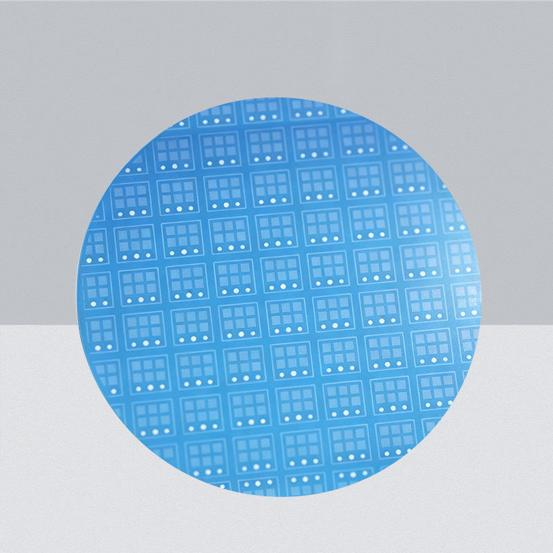
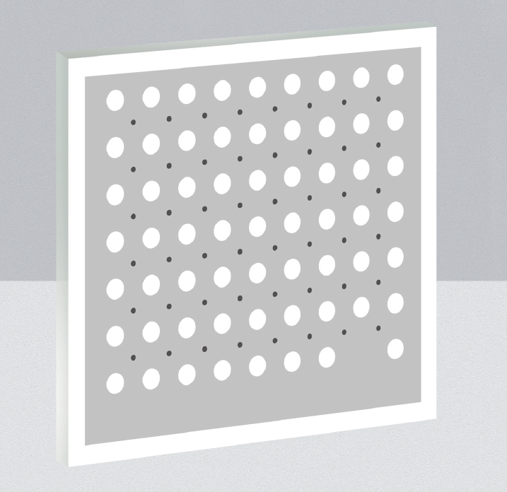
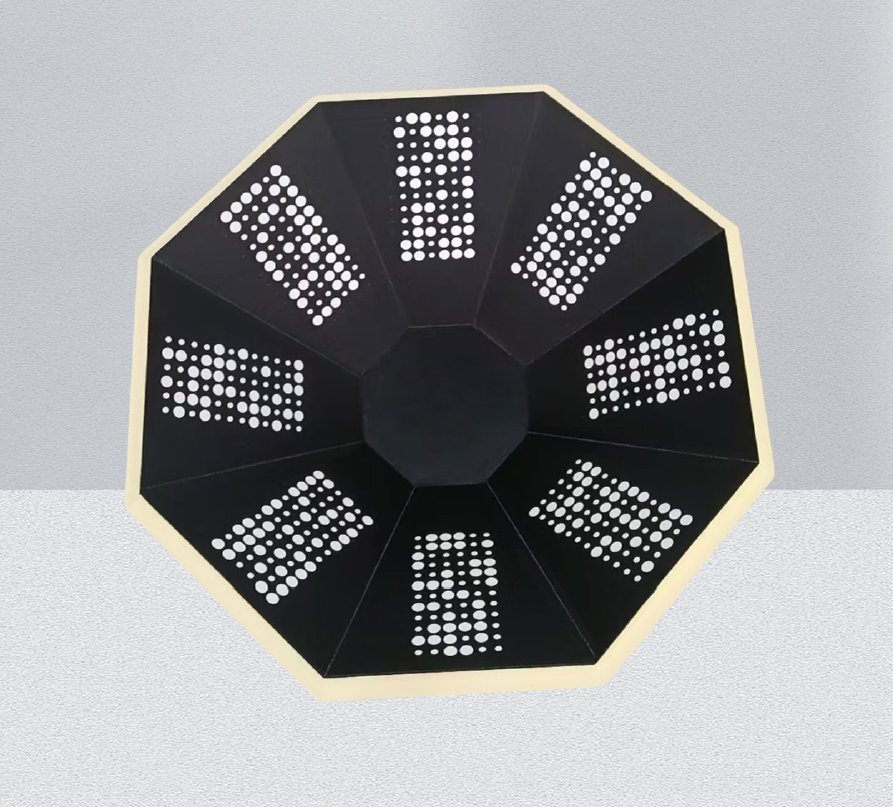
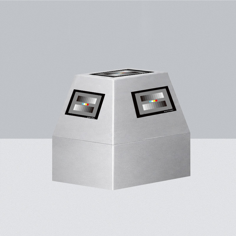
A wafer calibration board is a high-precision reference device used in semiconductor wafer inspection, measurement, and vision positioning systems. It provides reliable geometric dimensions, positions, angles, flatness, and optical parameter references for equipment by fabricating precisely calibrated standard patterns on a substrate. Simply put, the wafer calibration board is equivalent to the "standard ruler" and "reference coordinate system" for semiconductor equipment. The equipment measures the known and precise standard patterns on the calibration board, compares the actual measurement results with the standard values, thereby correcting equipment errors and improving measurement and positioning accuracy.


1. Common Structures

Wafer calibration boards typically use silicon wafers, glass, quartz, or other highly stable substrates with precisely patterned surfaces. Depending on the application, it includes:

(1) High-precision cross/mark marks

(2) Standard linewidth and spacing patterns

(3) Grid or array structures

(4) Standard-sized patterns such as circles and squares

(5) Test structures of different directions and scales

(6) Reference areas for height/flatness detection


2. Main Features

The main features of wafer calibration boards can be summarized as follows:

(1) High precision: The dimensions, spacing, and positions of the patterns on the calibration board are precisely machined and measured, providing a stable and reliable standard reference.

(2) High stability: Materials with good dimensional stability, such as silicon, quartz, and glass, are typically used, which can reduce dimensional changes caused by temperature, humidity, and long-term use.

(3) High flatness: The substrate surface has high flatness, which is beneficial to ensuring the accuracy of microscopic imaging, visual inspection, and height measurement.

(4) Pattern standardization: Different types of standard patterns can be designed according to equipment and application requirements, such as alignment marks, cross marks, linewidth/spacing structures, grids, and arrays. (5) Good Repeatability: The dimensions and patterns of the calibration board exhibit good repeatability, making it suitable for repeated measurements, accuracy verification, and long-term drift monitoring.

(6) Wide Applicability: It can be used in wafer inspection, AOI vision systems, microscopic measurement, wafer alignment, motion platform positioning, and optical system calibration.

(7) High Surface Quality: It typically requires low surface roughness and fewer defects and particles to minimize interference with optical inspection results.

(8) Customizable: The pattern size, layout, materials, and accuracy level can be customized according to wafer size, equipment accuracy, inspection magnification, and calibration items.


3. Main Application Areas of Wafer Calibration Boards

Wafer calibration boards are mainly used in semiconductor manufacturing, wafer inspection, optical measurement, and precision positioning, specifically including:

(1) Wafer Inspection Equipment

Used to calibrate equipment for wafer defect detection, dimensional inspection, and surface inspection, verifying the equipment's inspection accuracy, repeatability, and stability.

(2) Optical Microscopy Measurement

Applied to microscopes, optical measuring instruments, CD-SEM auxiliary systems, etc., for calibrating the magnification, pixel size, linewidth, and spacing of the equipment.

(3) Wafer Alignment and Positioning

Used in wafer alignment systems, vision positioning systems, and motion platforms, establishing accurate coordinate references through standard marks and other graphics to improve wafer positioning accuracy.

(4) Photolithography and Exposure Equipment

Used to verify the alignment accuracy, pattern position accuracy, and imaging effect of exposure equipment, assisting in equipment debugging and performance verification.

(5) Semiconductor Process Inspection

Used for pattern inspection after processes such as photolithography, etching, and thin film deposition, verifying linewidth, spacing, and pattern morphology through standard structures.

(6) Automated Optical Inspection (AOI) Systems

Used as a standard reference in wafer AOI and machine vision systems to calibrate cameras, lenses, light sources, and image algorithms, ensuring accurate inspection dimensions and positions.

(7) Precision Motion Platform

Used in wafer handling, inspection, and processing equipment to calibrate X/Y/Z axis motion accuracy, repeatability, and coordinate system.

(8) Equipment R&D and Acceptance

Used during semiconductor equipment R&D, installation, commissioning, and factory acceptance to verify whether the equipment meets the specified accuracy indicators and performance requirements.

(9) Scientific Research and Laboratory Metrology

Universities, research institutions, and semiconductor laboratories can use wafer calibration boards for optical system calibration, micro/nano-scale measurement, and accuracy verification of experimental equipment.

Send your message to this supplier
Send Now

Wafer Calibration Board Wafer Monitoring Calibration Target

Ask Latest Price
Certification :
ISO9001
Delivery Time :
10 work days
Payment Terms :
T/T
Customized Services :
Materials, specifications, precision, etc. can be customized
Supply Ability :
The average monthly production capacity for calibration plates and film is 300,000 pieces
Shipping Option :
FedEx And UPS
Contact Supplier
Wafer Calibration Board  Wafer Monitoring Calibration Target

Dongguan Dafan Optical Technology Co., Ltd.

Verified Supplier
1 Years
guangdong, dongguan
Since 2018
Business Type :
Manufacturer
Total Annual :
$12000000-$15000000
Employee Number :
120~150
Certification Level :
Verified Supplier
Contact Supplier
Submit Requirement